This is a document intended to describe the various hardware ports on the SNES. It will not describe how these ports are used by what may be plugged into them.
Controller Ports
The controller ports of the SNES has 7 pins, laid out something like this:
  ----------------------------- ---------------------
|                             |                      \
| (1)     (2)     (3)     (4) |   (5)     (6)     (7) |
|                             |                      /
  ----------------------------- ---------------------
| Pin | Description | Wire Color |
|---|---|---|
| 1 | +5v (power) | White |
| 2 | Clock | Yellow |
| 3 | Latch | Orange |
| 4 | Data1 | Red |
| 5 | Data2 | ? |
| 6 | IOBit | ? |
| 7 | Ground | Brown |
A standard controller has no wires for pins 5 and 6; these pins are used for non-standard controllers and controller splitters. Latch is written through bit 0 of register $4016. Writing 1 to this bit results in Latch going to whatever state means 'latch' to a joypad.
Clock of Port 1 is connected to the 'read' signal of $4016, in that reading $4016 causes Clock to transition. Data1 and Data2 are then read, and Clock transitions back (at this point, the pad is expected to stick its next bits of data on Data1 and Data2). Clock of Port 2 is connected to $4017.
Data1 and Data2 are read through bits 0 and 1 (respectively) of $4016 and $4017 (for Ports 1 and 2, respectively). Thus, you must read both bits at once, you can't choose to read only Data1 and leave Data2 for later.
IOBit is connected to the I/O Port (which is accessed through registers $4201 and $4213). Port 1's IOBit is connected to bit 6 of the I/O Port, and Port 2's IOBit is connected to bit 7. Note that, since bit 7 of the I/O Port is connected to the PPU Counter Latch, anything plugged into Port 2 may latch the H and V Counters by setting IOBit to 0.
Data1 and Data2 are pulled to logic-0 within the SNES, so reads will return 0 if nothing is plugged in.
Mouse Protocol
The SNES mouse uses the same timing and protocol as a regular pad for it's buttons. The left button is reported at the 9th cycle, and the right button at the 10th cycle. The SNES recognizes the mouse when the bit at the 16th clock cycle is low instead of high. 2.5ms after the 16 clock pulses, another series of clock pulses occurs. This is in fact cycles 17 to 32 since no new latch pulse had occurred yet. The data is active low, just like the buttons. This time, the clock timing is different:
                      8µs
                    -->|     |<--
                    .5µs
                  -->| |<--
data clock  --------   -----   -----   --/ /-  ...
                    | |     | |     | |     | |
                     -       -       -       -
                     17      18      19      32
Here is the meaning of the mouse specific cycles:
| Clock Cycle | Button Reported |
|---|---|
| 17 | Y direction (0=up, 1=down) |
| 18 | Y motion bit 6 |
| 19 | Y motion bit 5 |
| 20 | Y motion bit 4 |
| 21 | Y motion bit 3 |
| 22 | Y motion bit 2 |
| 23 | Y motion bit 1 |
| 24 | Y motion bit 0 |
| 25 | X direction (0=left, 1=right) |
| 26 | X motion bit 6 |
| 27 | X motion bit 5 |
| 28 | X motion bit 4 |
| 29 | X motion bit 3 |
| 30 | X motion bit 2 |
| 31 | X motion bit 1 |
| 32 | X motion bit 0 |
Each time the SNES polls the mouse, the mouse reports how it moved since last poll. When no movement occurred since last poll, all the motion bits stays high (which means binary 0). The direction bits keep their last state.
Mouse Sensitivity
The mouse has 3 configurable sensitivity levels. The currently active sensitivity level is reported by bits 11 and 12:
- Bit 11 low, Bit 12 high: High sensitivity
- Bit 11 high, Bit 12 low: Medium sensitivity
- Bit 11 high, Bit 12 high: Low sensitivity
Selecting the Sensitivity Mode
A special sequence is used to rotate between the 3 modes. First, a normal 12us latch pulse is applied. Next, the first 16 bits are read using normal button timings. Shortly after (about 1ms), 31 short latch pulses (3.4µS) are sent, with the clock going low for 700ns during each latch pulse. For selecting a specific sensitivity, simply execute the special sequence until bits 11 and 12 are as desired.
Cart Connector
The cart connector has 62 pads, laid out something like this:
                     +--------+
     21.477MHz Clock |  1  32 | /WRAM
              EXPAND |  2  33 | REFRESH
                 PA6 |  3  34 | PA7
               /PARD |  4  35 | /PAWR
                     |--------|
                 GND |  5  36 | GND
F                A11 |  6  37 | A12
r                A10 |  7  38 | A13
o                 A9 |  8  39 | A14
n                 A8 |  9  40 | A15
t                 A7 | 10  41 | A16
                  A6 | 11  42 | A17
o                 A5 | 12  43 | A18
f                 A4 | 13  44 | A19
                  A3 | 14  45 | A20
c                 A2 | 15  46 | A21
a                 A1 | 16  47 | A22
r                 A0 | 17  48 | A23
t               /IRQ | 18  49 | /CART
                  D0 | 19  50 | D4
                  D1 | 20  51 | D5
                  D2 | 21  52 | D6
                  D3 | 22  53 | D7
                 /RD | 23  54 | /WR
   CIC out data (p1) | 24  55 | CIC out data (p2)
    CIC in data (p7) | 25  56 | CIC in clock (p6)
              /RESET | 26  57 | CPU_CLOCK
                 Vcc | 27  58 | Vcc
                     |--------|
                 PA0 | 28  59 | PA1
                 PA2 | 29  60 | PA3
                 PA4 | 30  61 | PA5
    Left Audio Input | 31  62 | Right Audio Input
                     +--------+
A0-A23are the Address Bus A lines./WRand/RDare the associated read and write lines./WRAMis low when the CPU is accessing WRAM./CART, also called/ROMSEL, is low when the CPU is accessing ROM (banks$40-$7Dand$C0-$FF, or$8000-$FFFFof banks$00-$3Fand$80-$BF).
ROMSEL = (addr & 0x408000 == 0) || (addr & 0xFE0000 == 0x7E0000)
PA0-PA7are the Address Bus B lines, with/PARDand/PAWRthe associated read and write lines.D0-D7are the data bus lines.REFRESHis (presumably) the RAM refresh signal sent out each scanline for 40 master cycles.EXPANDis connected to pad 24 of the expansion port./IRQis connected to the CPU's/IRQline. This can be read by the cart, or activated by the cart to invoke an IRQ on the CPU./RESETis the reset signal, activated by the big reset button on the console. It can also be activated by hardware on the cart, if the system needs to be reset at a hardware level.CPU_CLOCKis (presumably) the current CPU cycle clock, which is either 6, 8, or 12 master cycles per cycle (3.58MHz, 2.68MHz, or 1.79MHz).
The signals input on Left and Right Audio Inputs are mixed into the APU's output audio.
The CIC pins are connected to the CIC chip, which is used for region lockouts. If the CIC in the console doesn't get the proper handshake over these pads, the reset signal is never released on the PPU2 chip, and so you never get anything on the display.
Many carts connect only to pins 5-27 and 36-58, as the remaining pins are mainly useful only if the cart contains special chips.
Expansion Port
The expansion port has 28 pads, laid out something like this. This pinout view faces the "cable" (i.e. expansion DEVICE socket). If you are looking at the port on the bottom of the console with the front of the console facing down, pin 1 is bottom-right and pin 28 is top-left.
               +--------+
           PA0 |  1   2 | PA1
           PA2 |  3   4 | PA3
           PA4 |  5   6 | PA5
           PA6 |  7   8 | PA7
         /PAWR |  9  10 | /PARD
            D0 | 11  12 | D1
            D2 | 13  14 | D3
            D4 | 15  16 | D5
            D6 | 17  18 | D7
        /RESET | 19  20 | Vcc
        SMPCLK | 21  22 | DOTCK
           GND | 23  24 | EXPAND
Mono Audio Out | 25  26 | /IRQ
 Left Audio In | 27  28 | Right Audio In
               +--------+
PA0-PA7are the Address Bus B lines, with/PARDand/PAWRthe associated read and write lines.D0-D7are the data bus lines./RESETis the reset signal, activated by the big reset button on the console. It can also be activated by hardware on the attached device, if the system needs to be reset at a hardware level.EXPANDis connected to pad 2 of the cart connector./IRQis connected to the CPU's /IRQ line. This can be read by the attached device, or activated by the attached device to invoke an IRQ on the CPU.- The signals input on Left and Right Audio Inputs are mixed into the APU's output audio. The (mono) audio output is brought back into pin 25.
SMPCLKandDOTCKare not really known.SMPCLKcomes from the audio subsystem; reports are that it's about 8.192MHz (i.e. 3 APU master clock cycles per cycle).DOTCKcomes from PPU2, and seems to be PPU dot clock at about 5.369 MHz (that's 21.477/4).
Multi-Out
The multi-out port has 12 pads, and looks something like this (2 version below):
   --------^--------
  /11  9  7  5  3  1\
 |                   |
  \12 10  8  6  4  2/
   -----------------
| Pin | Description |
|---|---|
| 1 | Red analog out |
| 2 | Green analog out |
| 3 | Composite H/V sync out () |
| 4 | Blue analog out |
| 5 | Ground |
| 6 | Ground |
| 7 | S-Video Y (luma) signal |
| 8 | S-Video C (chroma) signal |
| 9 | Composite video signal |
| 10 | Vcc |
| 11 | Mid sound (L+R) |
| 12 | Side sound (L-R) |
        1       3       5       7       9      11
        |       |       |       |       |       |
        |       |       |   _   |       |       |
       --------------------/ \--------------------
     /                                             \
    |                                               |
    |                                               |
     \                                             /
       -------------------------------------------
        |       |       |       |       |       |
        |       |       |       |       |       |
        2       4       6       8      10      12
| Pin | Description |
|---|---|
| 1 | Red analog video out (1v DC offset, 1vpp video into 75 ohms) |
| 2 | Green analog video out (1v DC offset, 1vpp video into 75 ohms) |
| 3 | Composite H/V sync out (1vpp into 75 ohms) |
| 4 | Blue analog video out (1v DC offset, 1vpp video into 75 ohms) |
| 5 | Ground |
| 6 | Ground |
| 7 | Y (luma) signal for S-Video (1vpp into 75 ohms) |
| 8 | C (chroma) signal for S-Video (1vpp into 75 ohms) |
| 9 | Composite video signal (1vpp into 75 ohms) |
| 10 | Vcc / +5v (Could be a high logic signal or power for an external RF modulator) |
| 11 | Left channel audio out |
| 12 | Right channel audio out |
RF Out
I know nothing about the output of this port, except that it has a Vcc, a GND, a video signal, and a mono audio signal.
Power
This one is simple. It's a barrel connector, a hollow cylindrical plug. It expects to be supplied with DC 10V, 850mA DC power source. The US power adapter produces centre-negative DC. At least on PAL units (SNSP), the DC jack can be fed with centre-positive or centre-negative as there is a AC-DC converter inside.
ROM Pinout
This seems to be consistent with both mask ROMs, some are 32pin, others 36pin.
32PIN MaskROM
=============
A17   01         32   Vcc
A18   02         31   /OE
A15   03         30   A19
A12   04         29   A14
 A7   05         28   A13
 A6   06         27   A8
 A5   07         26   A9
 A4   08         25   A11
 A3   09         24   A16
 A2   10         23   A10
 A1   11         22   /CS
 A0   12         21   D7
 D0   13         20   D6
 D1   14         19   D5
 D2   15         18   D4
Vss   16         17   D3

36PIN MaskROM
=============
A20   01         36   Vcc
A21   02         35   A22
A17   03         34   Vcc
A18   04         33   /OE
A15   05         32   A19
A12   06         31   A14
 A7   07         30   A13
 A6   08         29   A8
 A5   09         28   A9
 A4   10         27   A11
 A3   11         26   A16
 A2   12         25   A10
 A1   13         24   /CS
 A0   14         23   D7
 D0   15         22   D6
 D1   16         21   D5
 D2   17         20   D4
Vss   18         19   D3
DSP Pinout
This is how most DSP chips are hooked up. DSP is a uPD77C25 made by NEC.
 Vcc   01   28   Vcc
 Vcc   02   27   register select(A14 used when DSP is mapped to cartridge memory region,
  NC   03   26   /CS             A12 used when DSP is mapped to expansion memory region)
  NC   04   25   /RD
  NC   05   24   /WR
  D0   06   23   NC
  D1   07   22   NC
  D2   08   21   Vcc
  D3   09   20   Vcc
  D4   10   19   Vcc
  D5   11   18   Vcc
  D6   12   17   GND
  D7   13   16   RESET (inverted /RESET- SNES slot)
 GND   14   15   CLOCK
MAD-1 Pinout
The MAD-1 stands for Memory Address Decoder revision 1. It is used for memory mapping in both HiROM and LoROM. And is used for battery power control on a static RAM.
                           /HI  01      16  /LOW
                      SRAM /CS  02      15  A15 (LoROM), A13 (HiROM)
                            NC  03      14  BA4 (LoROM), A14 (HiROM)
                       ROM /OE  04      13  BA5
                      SRAM Vcc  05      12  Vcc or BA6 (LoROM), A15 or BA6(HiROM)...
                           Vcc  06      11  /CART (pad 49 on cartridge edge)
    resistor to +3V of battery  07      10  GND=LoROM, Vcc=HiROM
                           GND  08      09  /RESET (pad 26 on cartridge edge)

    /HI <--- if two ROM chips, this selects the upper one
    /LOW <--- if two ROM chips, this selects the lower one

    Verified & Simplified by kyuusaku
    Pin  9 is A
    Pin 10 is B
    Pin 11 is C
    Pin 12 is D
    Pin 13 is E
    Pin 14 is F
    Pin 15 is G

    The Logic (Invert Outputs)
    ==========================
    Pin  1 is G E C' A + E C' B A
    Pin  2 is G F E D' C B A + G' F E D C' B' A + SRAMVCC'
    Pin  3 is G F E' D' C B A + G' F' E D C' B' A
    Pin  4 is G C' A + C' B A
    Pin 16 is G E' C' A + E' C' B A
CIC Lockout Chip / Security Chip
The infamous CIC. Variants include D411, D411A, D411B, F411A, D413, D413A, D413B and F413A.
pad24  01      16  Vcc
pad55  02      15  NC
   NC  03      14  NC
  GND  04      13  NC
   NC  05      12  NC
pad56  06      11  NC
pad25  07      10  NC
  GND  08      09  NC
SRAM Pinouts
16kbit SRAM
=========================
 A7   01         24   Vcc
 A6   02         23   A8
 A5   03         22   A9
 A4   04         21   /WE
 A3   05         20   /OE
 A2   06         19   A10
 A1   07         18   /CS
 A0   08         17   D7
 D0   09         16   D6
 D1   10         15   D5
 D2   11         14   D4
Vss   12         13   D3

256kbit SRAM (HY62256ALLP-10)
=============================
  A14   01         28   Vcc
  A12   02         27   /WE
   A7   03         26   A13
   A6   04         25   A8
   A5   05         24   A9
   A4   06         23   A11
   A3   07         22   /OE
   A2   08         21   A10
   A1   09         20   /CS
   A0   10         19   D7
   D0   11         18   D6
   D1   12         17   D5
   D2   13         16   D4
  GND   14         15   D3
RGB Monitors
This section covers commonly used monitors and displays used in conjunction with the Super NES or Super Famicom or generally used in retro gaming.
Casio CMV54NT04P / Sharp LM6Q401
This is the Casio (カシオ) 5.4 inch screen (sometimes written as Casio CMV54NTO4P) used in the Interact GameCube LCD screens, Iomega XBOX screens and a number of portable console mods. You can see it in action with various consoles and computers here. It can run off a standard NES power supply. Below is a pinout for the back 10-pin connection, it is clearly labeled on the PCB which pins are 1 and 6.
--^-----------^--
| 1  2  3  4  5 |
| 6  7  8  9 10 |
-----------------
| Pin | Description |
|---|---|
| 1 | Screen Rotation |
| 2 | Blue |
| 3 | Red |
| 4 | +12V |
| 5 | Ground |
| 6 | Screen Flip |
| 7 | Composite Sync |
| 8 | Green |
| 9 | +12V |
| 10 | Brightness |
In order to use a Japanese SCART with this it requires the use of a LM1881 Chip as seen below.
LM1881 Chip - Video Sync Separator
Most game systems output the composite sync information along with the NTSC video output. Many RGB displays will not accept this extraneous info along with the sync, so we need to remove the video signal. The LM1881 / LM1881N does just this. It's a simple circuit - one small chip, two small capacitors and a small resistor. Download LM1881N_Datasheet.pdf.
----\/----
| 1    8 |
| 2    7 |
| 3    6 |
| 4    5 |
----------
| Pin | Description |
|---|---|
| 1 | Composite Sync Output |
| 2 | Composite Video Input |
| 3 | Vertical Sync Output |
| 4 | Ground (?) |
| 5 | Burst / Back Porch Output |
| 6 | R-Set |
| 7 | Odd / Even Output |
| 8 | VCC 5-12V |
Japanese 21-pin RGB Connector
This is the Japanese RGB connector used on many video game systems. It is physically identical to the European SCART / Péritel / Euroconnector with a different pinout.
    |------------------------------------------|
    |   2   4   6   8  10  12  14  16  18  20  |
    |                                         / 21
    | 1   3   5   7   9  11  13  15  17  19  |
    |-----------------------------------------

     1: Audio Left Channel Input     2: Audio Left Channel Output
     3: Audio Ground                 4: Audio Ground
     5: Audio Right Channel Input    6: Audio Right Channel Output
     7: Sync / Video Ground          8: Video Ground
     9: Sync / CVBS Input           10: CVBS Output
    11: AV Control Input / +5V      12: Ym Input
    13: Red Signal Ground           14: Ground
    15: Red Signal I/O              16: Ys Input / 1V
    17: Green Signal Ground         18: Blue Signal Ground
    19: Green Signal I/O            20: Blue Signal I/O
    21: Plug Shield / Ground
Special Notes:
- Connect pin 16 to pin 11 via 3.3k Ohm resistor. The resistor isn't usually necessary, and +5V on this pin will most often work.
- Audio Input: 0.40 mVrms, > 47K ohms
- Audio Output: 0.40 mVrms, > 10K ohms
- CVBS (Composite Video) in and out: 1 Vp-p, 75 ohms, sync: negative
- Ym Input: Switches RGB to half-brightness, for video overlay (L: < 0.4V, H: > 1V, 75 ohms)
- Ys Input: RGB in/out: (Ground for output, 1V+ for Input (preferred)1))
- All RGB lines: 0.7 Vp-p, 75 ohms
SNES Schematic
In the doc below, "active", "1", "logic-1", and so forth all mean the same thing. Note that "1" does not necessarily correspond to either high or low voltage. (BTW, I could use some help here: if anyone knows whether anything is active-high or active-low, or what the voltages for high and low are for any particular port, please let me know!)
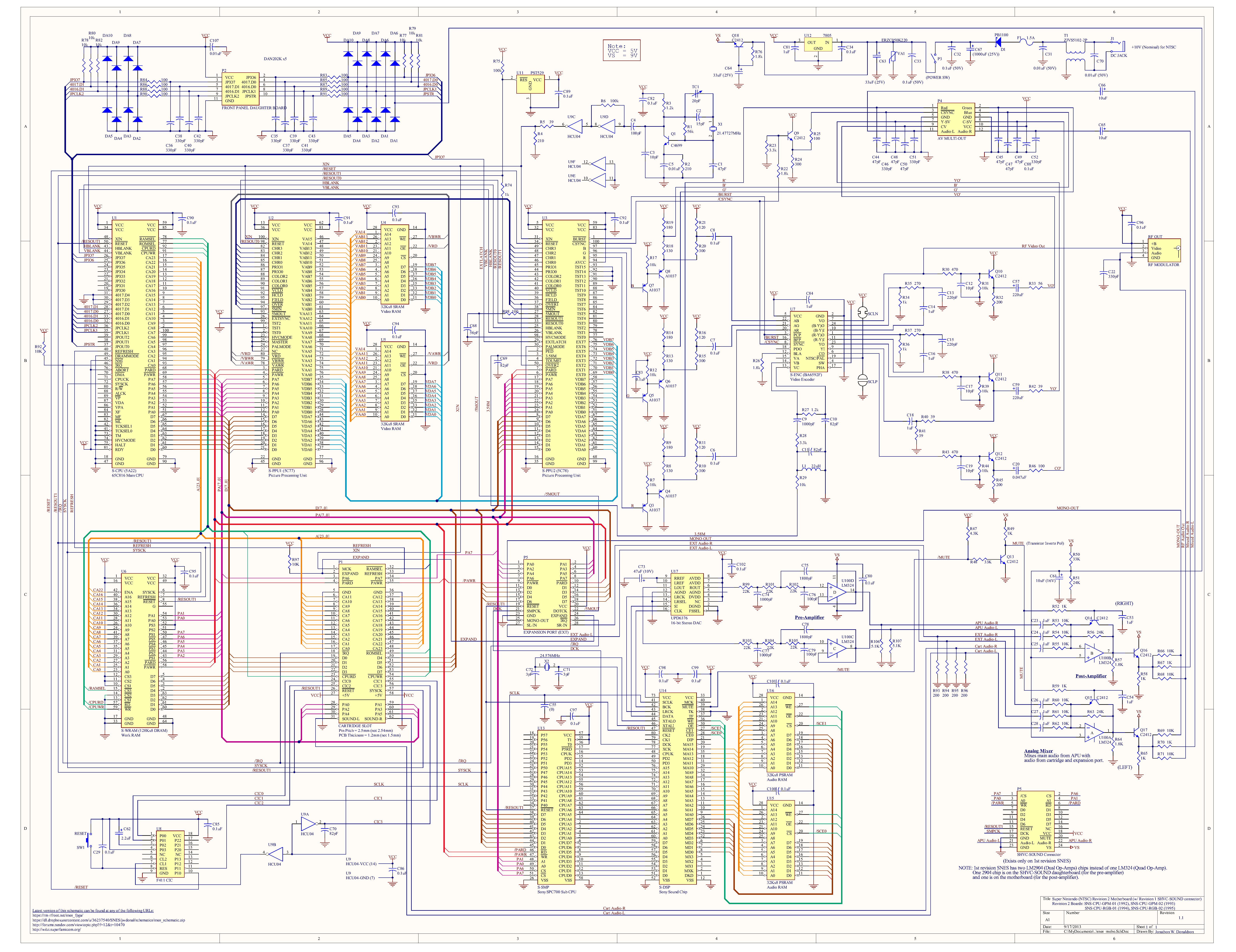
By Anomie (anomie@users.sourceforge.net), jwdonal, and Others