System Overview
CPU
8-bit SPC700, runs at 1.024MHz, however, each instruction takes a minimum of 2 cycles
Memory
64KB (NOT 32KB), shared with everything.
Communication
4 8-bit I/O ports to transfer data to/from the SNES.
Sound
8x channels of ADPCM compressed sample goodness. The DSP also has special hardware for echo effects, white noise, and pitch modulation.
Timers
Two 8-bit 8KHz timers + one more 8-bit 64KHz timer, all have 4-bit count-up values.
SPC Memory Map and Registers
| Range | Description |
|---|---|
0000 - 00EF |
Page 0 |
00F0 - 00FF |
Registers |
0100 - 01FF |
Page 1 |
0200 - FFBF |
Memory |
FFC0 - FFFF |
Memory (read / write) |
FFC0 - FFFF |
Memory (write only)* |
FFC0 - FFFF |
64 byte IPL ROM (read only)* |
* Only if X bit is set in the undocumented register.
Pages 0/1 are known as the "Zero Pages". Accesses to zero page memory can be done with faster (and smaller) cpu instructions (one byte addresses). Which zero page to be operated on can be switched with a processor flag. Page 1 is mainly used for stack space.
Registers
| Mnemonic | Description | Control |
|---|---|---|
F0 |
Undocumented | ?/W |
F1 |
Control Register | /W |
F2 |
DSP Register Address | R/W |
F3 |
DSP Register Data | R/W |
F4 |
Port 0 | R/W |
F5 |
Port 1 | R/W |
F6 |
Port 2 | R/W |
F7 |
Port 3 | R/W |
F8 |
Regular Memory | R/W |
F9 |
Regular Memory | R/W |
FA |
Timer-0 | /W |
FB |
Timer-1 | /W |
FC |
Timer-2 | /W |
FD |
Counter-0 | R/ |
FE |
Counter-1 | R/ |
FF |
Counter-2 | R/ |
Control Register
       7     6     5     4     3     2     1     0
    +-----+-----+-----+-----+-----+-----+-----+-----+
 F1 |  -  |  -  | PC32| PC10|  -  | ST2 | ST1 | ST0 | Control, Write only!
    +-----+-----+-----+-----+-----+-----+-----+-----+

PC32: "PORT CLEAR" Writing '1' here will reset input from ports 2 & 3. (reset to zero)
PC10: "PORT CLEAR" Writing '1' here will reset input from ports 0 & 1.
STx:  Writing '1' here will activate timer X, writing '0' disables the timer.
There will probably be some conflict if the snes writes data at the same time the SPC initiates a port clear function.
Some emulators don't emulate this, BSNES does though.
Writing to the control register will ALWAYS reset active timers. Control is not readable. Writing '1' to any of the timer bits will start / restart the timer, even if it's already active, writing '0' will stop the timer. Even when using bit operations, the other timers will still be affected.
Communication Ports
There are 8 bytes worth of buffered data passed around; one byte on the SPC side and one byte on the CPU side, for each of the 4 ports. Therefore, data can be written in both directions simultaneously. The SNES uses registers 2140 - 2143. The SPC uses registers F4 - F7.
SNES SIDE               SPC SIDE

(write)                    (write)
-----> $2140 ------------,    .-------- $F4 <-----
-----> $2141 ----------, |    | .------ $F5 <-----
-----> $2142 --------, | |    | | .---- $F6 <-----
-----> $2143 ------, | | |    | | | .-- $F7 <-----
                   | | | |    | | | |
<----- $2140 <-----|-|-|-|----' | | |
<----- $2141 <-----|-|-|-|------' | |
<----- $2142 <-----|-|-|-|--------' |
<----- $2143 <-----|-|-|-|----------'
 (read)            | | | |          (read)
                   | | | `------------> $F4 ------>
                   | | `--------------> $F5 ------>
                   | `----------------> $F6 ------>
                   `------------------> $F7 ------>
Hardware Quirk! When writing in 16-bit values to 2140 / 2141, a noise pulse (or some technical thingy) may write data to 2143 too! Always write to 2140 / 2141 with 8-bit writes if this is undesired.
Another Warning! When a read from a port conflicts with a write to the port from the opposing CPU, the data may be garbled. Always re-fetch values that may be affected by this conflict!
Here is a fraction of code that handles the above conflict:
;-------------------------------------------------------------------
comms_process:
;-------------------------------------------------------------------

    mov a, comms_v          ; COMMS_V is the last data written to port0
    cmp a, spc_port0        ; if the value in port0 is different, this means the SNES has sent new data.
    beq cp_exit             ; if its the same, then there are no messages.

; receive message
    mov a, spc_port1        ; PORT1 contains the message type
    mov comms_v, spc_port0  ; PORT0 should contain valid data now, since a few cycles have passed.
    cmp a, #20h             ; determine message type... etc...

    --PROCESS MESSAGE--

    mov spc_port0, comms_v  ; mimic the value of port0 to let the SPC know we're finished,
                            ; if the value is incorrect then the SNES will get caught in an infinite loop.
Here is an unstable example that may crash:
;-------------------------------------------------------------------
comms_process:
;-------------------------------------------------------------------

    mov a, spc_port0        ; check port0 for different data
    cmp a, comms_v          ; comms_v is last value
    beq cp_exit             ; if its the same, then there are no messages.

; receive message
    mov comms_v, a          ; save validation <- THE DATA MAY BE GARBLED!
    mov a, spc_port1

    --PROCESS MESSAGE--

    mov spc_port0, comms_v  ; mimic the value of port0 to let the blah blah blah. This
                            ; data might be incorrect! It may hang-up the SNES side.
DSP Access
The DSP is accessed through 2 registers. One register points to a DSP register index. The other allows reading from / writing to the DSP register specified.
         7     6     5     4     3     2     1     0
      +-----+-----+-----+-----+-----+-----+-----+-----+
$F2   |  x  |  x  |  x  |  x  |  x  |  x  |  x  |  x  | DSP-Address, Read / Write
      +-----+-----+-----+-----+-----+-----+-----+-----+

x: Pointer to DSP register.

         7     6     5     4     3     2     1     0
      +-----+-----+-----+-----+-----+-----+-----+-----+
$F3   |  x  |  x  |  x  |  x  |  x  |  x  |  x  |  x  | DSP-Data, Read / Write
      +-----+-----+-----+-----+-----+-----+-----+-----+

x: Data to be written / data being read.
To write a value to the DSP:
- Write address of DSP register to
F2. - Write desired value to
F3.
And to read a value:
- Write address of DSP register to
F2. - Read the value from
F3.
F2 / F3 can be written simultaneously with a 16-bit transfer:
; Setting DSP register $00 to $25
; and $01 to $30

    mov a, #$00
    mov y, #$25
    movw    $F2, ya
    inc a
    mov y, #$30
    movw    $F2, ya

; theres a few possibilities to write data to the DSP...
; spc has some mem->mem / mem->imm instructions too.
    inc $F2     ; set register $02 to $99
    mov $F3, #$99
Timers
The SPC contains 3 timers that can be used for general purpose. Timers 0,1 count up at 8KHz, Timer 2 has a higher precision of 64KHz.
         7     6     5     4     3     2     1     0
      +-----+-----+-----+-----+-----+-----+-----+-----+
$FA+X |  t  |  t  |  t  |  t  |  t  |  t  |  t  |  t  | Timer-X, Write only!
      +-----+-----+-----+-----+-----+-----+-----+-----+

t: Timing value.

         7     6     5     4     3     2     1     0
      +-----+-----+-----+-----+-----+-----+-----+-----+
$FD+X |  -  |  -  |  -  |  -  |  c  |  c  |  c  |  c  | Counter-X, Read only!
      +-----+-----+-----+-----+-----+-----+-----+-----+

c: Count-up value.
The timers consist of an 8-bit internal counter and a 4-bit up-counter. When the timer is off, the internal counter can be programmed through registers Timer-X registers. When the timer is activated by a '1' bit in the Control register, then the timer starts counting up (at 8KHz/64Khz) until it reaches the amount specified in Timer-X. When this happens the internal counter is reset and Counter-X is incremented. When you read Counter-X, the value in it will be reset to zero. Take care not to let the up-counter overflow! It's only 4-bits wide, and if it overflows the value will be lost.
Psuedo Code - Setting Timer 0 to tick at 15ms:
- ...Make sure the timer is off.
- Write 120 (0x78) to
FA(15/(1000/8000) = 15*8 = 120) - Write '1' to the control register bit (
F1) - Timer is started..
- Read
FDperiodically to check if ticks have passed.
Real Code:
; An example to wait 15ms.

    mov timer0,  #$78           ; 15ms timing value
    mov control, #$01           ; this will destroy all other timers

    ; timer is started

wait_for_tick:
        mov a, counter0         ; read counter
        beq     wait_for_tick   ; loop if 0

    ; tick has passed, process data
CPU Register Set
The CPU has 6 registers in it: A, X, Y, SP, PC, PSW
All are 8-bit except for the PC (Program Counter), which points at a 16-bit program execution address.
The A (Accumulator) register is compatible with most CPU instructions.
The X/Y (Index) registers are mostly used for counters/memory addressing. For some instructions, the Y register can be paired with A ("YA") for 16-bit operations.
The SP (Stack Pointer) register points to an area of memory in Page1 (0100 - 01FF). Stack operations affect SP, the IPL ROM initializes SP to the top of Page1.
The PSW (Program Status Word) register contains various bits that effect operation of the CPU.
CPU Program Status Word
Flags stored in PSW Register
| Mnemonic | Description |
|---|---|
N |
Negative |
V |
Overflow |
P |
Direct page |
B |
Break |
H |
Half Carry |
I |
Interrupt enabled (unused) |
Z |
Zero |
C |
Carry |
Negative Flag (N): The MSB of an operation's result is copied to the Negative flag.
Overflow Flag (V): I don't think I ever had to use this bit, It tells you if an overflow occured in the previous arithmetic operation.
Direct Page Flag (P): This bit controls the direct-page (dp) operations. The dp operations only have 1 address byte. If the P flag is cleared then the effective address will be 0000h+address. Otherwise it will be 0100h+address.
Half Carry Flag (H): The half-carry flag is used in arithmetic operations. It can be used to determine if the DAA/DAS instruction needs to be executed after a BCD addition/subtraction operation. It cannot be directly set by any instruction, however, it is cleared with CLRV.
Carry Flag (C): The carry flag is mainly used in arithmetic operations. It can be used to control program flow after addition/subtraction. Its also used by a few other functions, like shift commands. It can be directly set by instructions SETC and CLRC.
Break Flag (B): This flag is unused. The only instruction that touches it is BRK.
Interrupt Enable (I): Interrupts are not supported. This flag is unused.
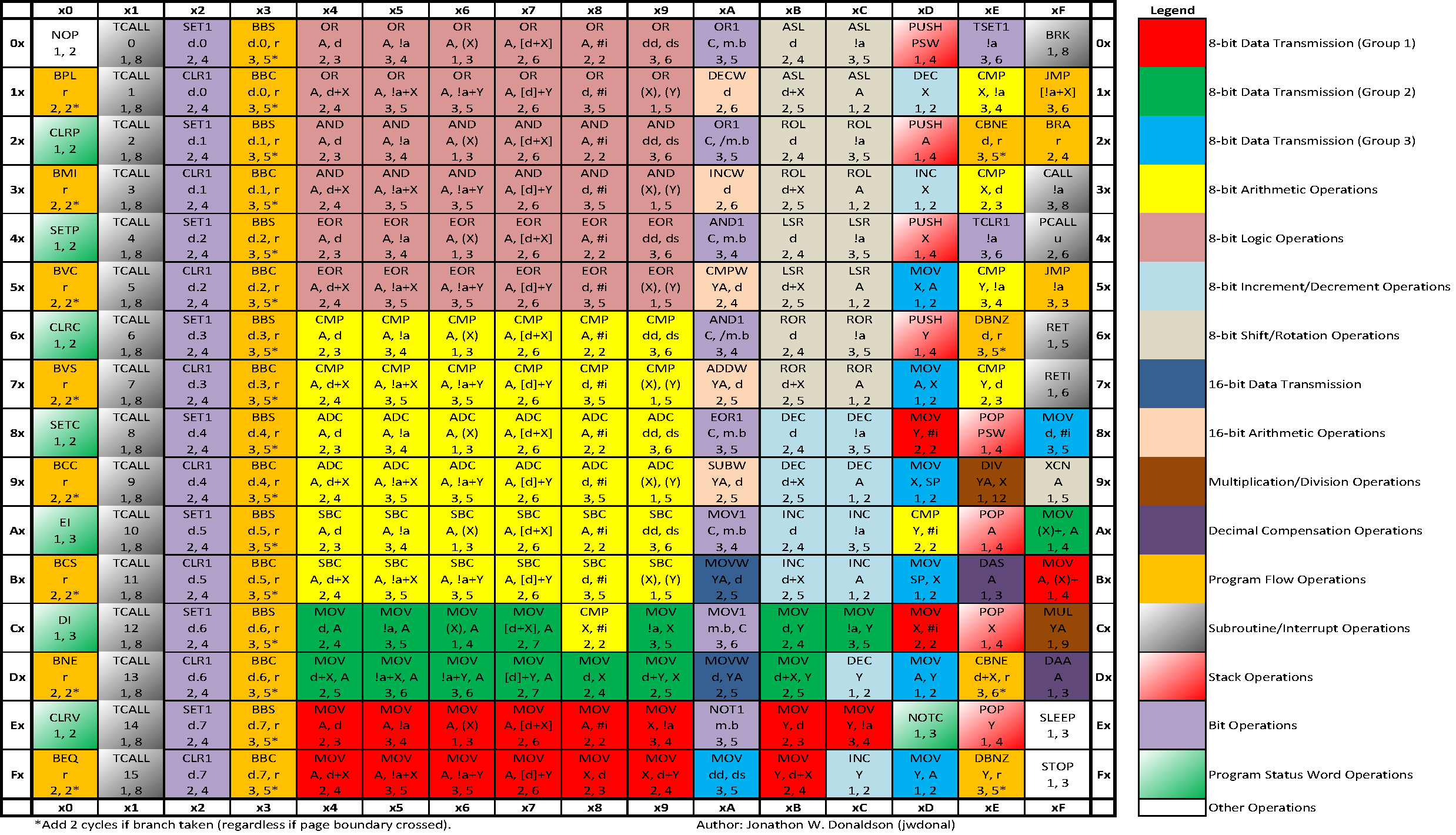
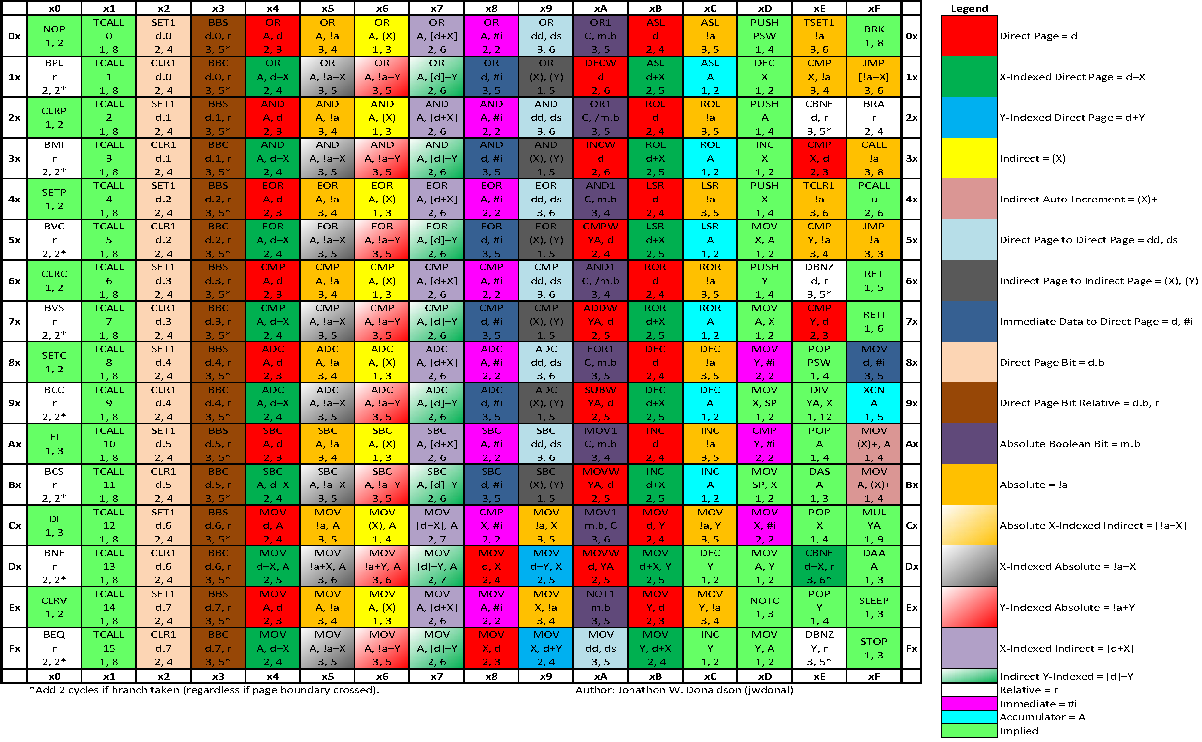
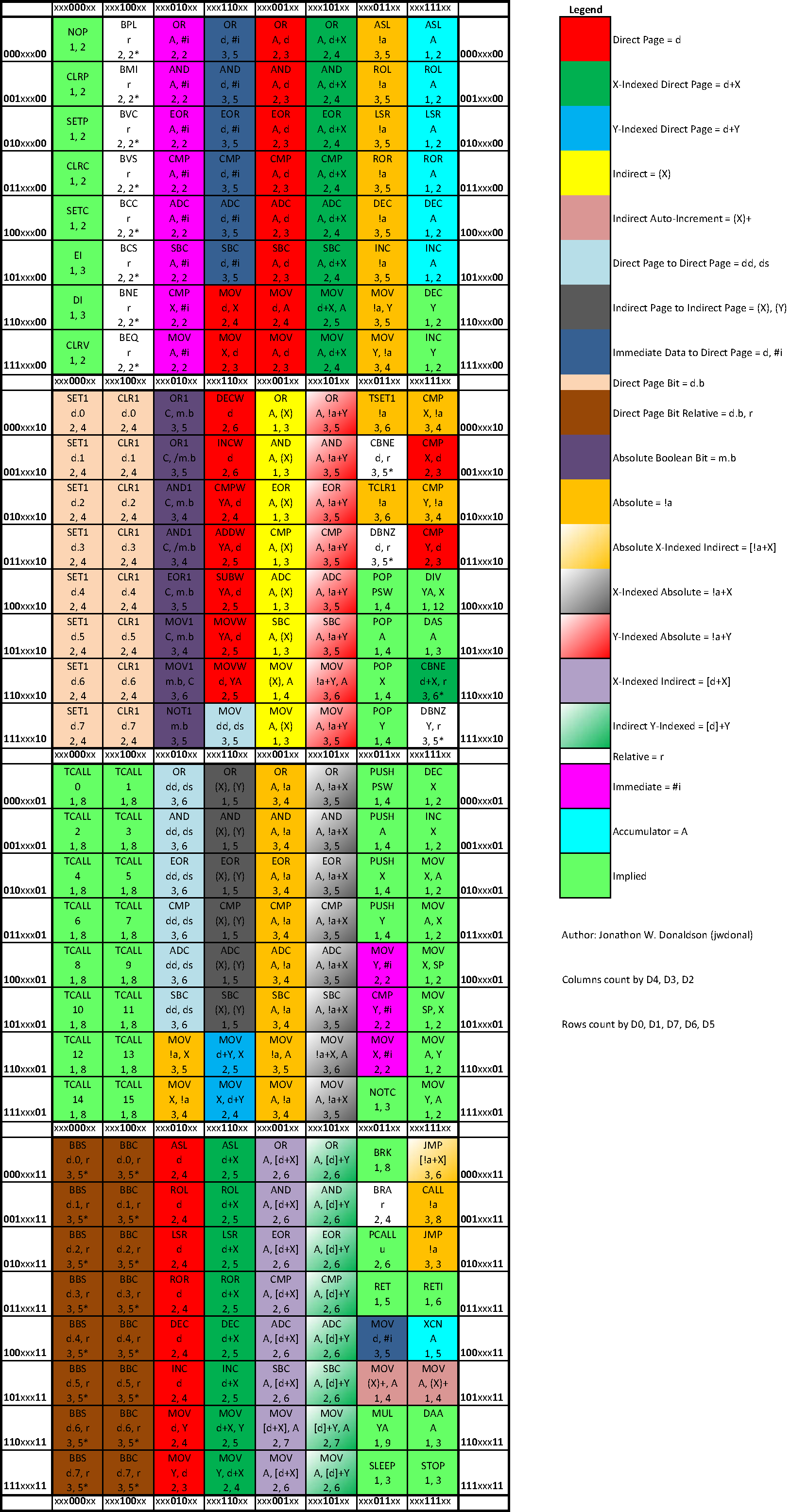
Opcode Matrices (by jwdonal)
SPC700 Opcode Matrix by Type (Native Mnemonics)
SPC700 Opcode Matrix by Type (65816-Style Mnemonics)

SPC700 Opcode Matrix by Addressing Mode (Native Mnemonics)
SPC700 Opcode Matrix by Addressing Mode (65816-Style Mnemonics)

SPC700 Opcode Matrix by Bits (Native Mnemonics)
SPC700 Opcode Matrix by Bits (65816-Style Mnemonics)

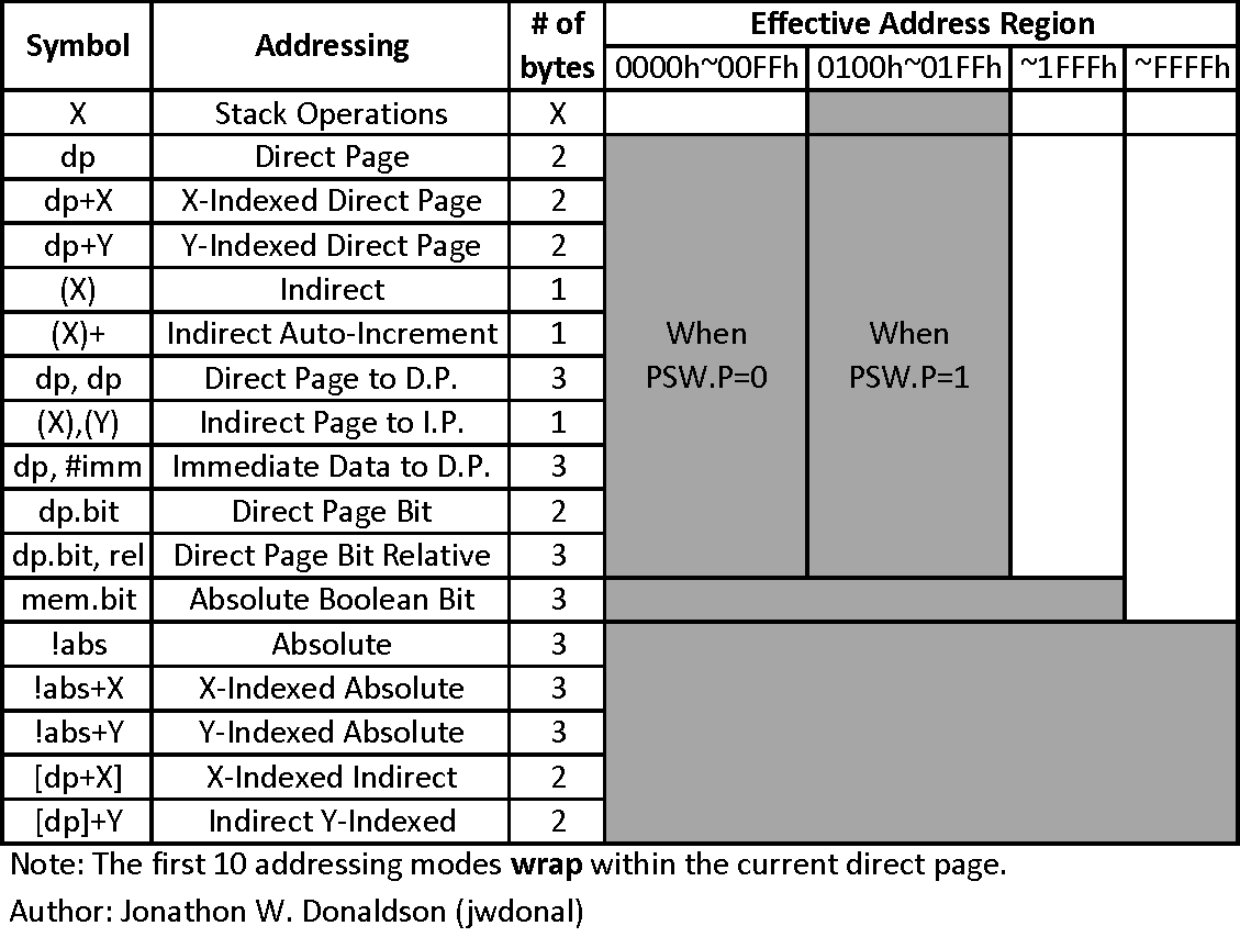
SPC700 Addressing Modes Effective Address Regions
Instruction Chart
| Assembler Example | Operation | HEX | Flags Set | Bytes | Cycles |
|---|---|---|---|---|---|
ADC (X), (Y) |
(X) = (X)+(Y)+C |
99 | NV--H-ZC | 1 | 5 |
ADC A, #i |
A = A+i+C |
88 | NV--H-ZC | 2 | 2 |
ADC A, (X) |
A = A+(X)+C |
86 | NV--H-ZC | 1 | 3 |
ADC A, [d]+Y |
A = A+([d]+Y)+C |
97 | NV--H-ZC | 2 | 6 |
ADC A, [d+X] |
A = A+([d+X])+C |
87 | NV--H-ZC | 2 | 6 |
ADC A, d |
A = A+(d)+C |
84 | NV--H-ZC | 2 | 3 |
ADC A, d+X |
A = A+(d+X)+C |
94 | NV--H-ZC | 2 | 4 |
ADC A, !a |
A = A+(a)+C |
85 | NV--H-ZC | 3 | 4 |
ADC A, !a+X |
A = A+(a+X)+C |
95 | NV--H-ZC | 3 | 5 |
ADC A, !a+Y |
A = A+(a+Y)+C |
96 | NV--H-ZC | 3 | 5 |
ADC dd, ds |
(dd) = (dd)+(d)+C |
89 | NV--H-ZC | 3 | 6 |
ADC d, #i |
(d) = (d)+i+C |
98 | NV--H-ZC | 3 | 5 |
ADDW YA, d |
YA = YA + (d), H on high byte |
7A | NV--H-ZC | 2 | 5 |
AND (X), (Y) |
(X) = (X) & (Y) |
39 | N-----Z- | 1 | 5 |
AND A, #i |
A = A & i |
28 | N-----Z- | 2 | 2 |
AND A, (X) |
A = A & (X) |
26 | N-----Z- | 1 | 3 |
AND A, [d]+Y |
A = A & ([d]+Y) |
37 | N-----Z- | 2 | 6 |
AND A, [d+X] |
A = A & ([d+X]) |
27 | N-----Z- | 2 | 6 |
AND A, d |
A = A & (d) |
24 | N-----Z- | 2 | 3 |
AND A, d+X |
A = A & (d+X) |
34 | N-----Z- | 2 | 4 |
AND A, !a |
A = A & (a) |
25 | N-----Z- | 3 | 4 |
AND A, !a+X |
A = A & (a+X) |
35 | N-----Z- | 3 | 5 |
AND A, !a+Y |
A = A & (a+Y) |
36 | N-----Z- | 3 | 5 |
AND dd, ds |
(dd) = (dd) & (ds) |
29 | N-----Z- | 3 | 6 |
AND d, #i |
(d) = (d) & i |
38 | N-----Z- | 3 | 5 |
AND1 C, /m.b |
C = C & ~(m.b) |
6A | -------C | 3 | 4 |
AND1 C, m.b |
C = C & (m.b) |
4A | -------C | 3 | 4 |
ASL A |
Left shift A: high->C, 0->low |
1C | N-----ZC | 1 | 2 |
ASL d |
Left shift (d) as above |
0B | N-----ZC | 2 | 4 |
ASL d+X |
Left shift (d+X) as above |
1B | N-----ZC | 2 | 5 |
ASL !a |
Left shift (a) as above |
0C | N-----ZC | 3 | 5 |
BBC d.0, r |
PC+=r if d.0 == 0 |
13 | -------- | 3 | 5/7 |
BBC d.1, r |
PC+=r if d.1 == 0 |
33 | -------- | 3 | 5/7 |
BBC d.2, r |
PC+=r if d.2 == 0 |
53 | -------- | 3 | 5/7 |
BBC d.3, r |
PC+=r if d.3 == 0 |
73 | -------- | 3 | 5/7 |
BBC d.4, r |
PC+=r if d.4 == 0 |
93 | -------- | 3 | 5/7 |
BBC d.5, r |
PC+=r if d.5 == 0 |
B3 | -------- | 3 | 5/7 |
BBC d.6, r |
PC+=r if d.6 == 0 |
D3 | -------- | 3 | 5/7 |
BBC d.7, r |
PC+=r if d.7 == 0 |
F3 | -------- | 3 | 5/7 |
BBS d.0, r |
PC+=r if d.0 == 1 |
03 | -------- | 3 | 5/7 |
BBS d.1, r |
PC+=r if d.1 == 1 |
23 | -------- | 3 | 5/7 |
BBS d.2, r |
PC+=r if d.2 == 1 |
43 | -------- | 3 | 5/7 |
BBS d.3, r |
PC+=r if d.3 == 1 |
63 | -------- | 3 | 5/7 |
BBS d.4, r |
PC+=r if d.4 == 1 |
83 | -------- | 3 | 5/7 |
BBS d.5, r |
PC+=r if d.5 == 1 |
A3 | -------- | 3 | 5/7 |
BBS d.6, r |
PC+=r if d.6 == 1 |
C3 | -------- | 3 | 5/7 |
BBS d.7, r |
PC+=r if d.7 == 1 |
E3 | -------- | 3 | 5/7 |
BCC r |
PC+=r if C == 0 |
90 | -------- | 2 | 2/4 |
BCS r |
PC+=r if C == 1 |
B0 | -------- | 2 | 2/4 |
BEQ r |
PC+=r if Z == 1 |
F0 | -------- | 2 | 2/4 |
BMI r |
PC+=r if N == 1 |
30 | -------- | 2 | 2/4 |
BNE r |
PC+=r if Z == 0 |
D0 | -------- | 2 | 2/4 |
BPL r |
PC+=r if N == 0 |
10 | -------- | 2 | 2/4 |
BVC r |
PC+=r if V == 0 |
50 | -------- | 2 | 2/4 |
BVS r |
PC+=r if V == 1 |
70 | -------- | 2 | 2/4 |
BRA r |
PC+=r |
2F | -------- | 2 | 4 |
BRK |
Push PC and Flags, PC = [$FFDE] |
0F | ---1-0-- | 1 | 8 |
CALL !a |
(SP--)=PCh, (SP--)=PCl, PC=a |
3F | -------- | 3 | 8 |
CBNE d+X, r |
CMP A, (d+X) then BNE |
DE | -------- | 3 | 6/8 |
CBNE d, r |
CMP A, (d) then BNE |
2E | -------- | 3 | 5/7 |
CLR1 d.0 |
d.0 = 0 |
12 | -------- | 2 | 4 |
CLR1 d.1 |
d.1 = 0 |
32 | -------- | 2 | 4 |
CLR1 d.2 |
d.2 = 0 |
52 | -------- | 2 | 4 |
CLR1 d.3 |
d.3 = 0 |
72 | -------- | 2 | 4 |
CLR1 d.4 |
d.4 = 0 |
92 | -------- | 2 | 4 |
CLR1 d.5 |
d.5 = 0 |
B2 | -------- | 2 | 4 |
CLR1 d.6 |
d.6 = 0 |
D2 | -------- | 2 | 4 |
CLR1 d.7 |
d.7 = 0 |
F2 | -------- | 2 | 4 |
CLRC |
C = 0 |
60 | -------0 | 1 | 2 |
CLRP |
P = 0 |
20 | --0----- | 1 | 2 |
CLRV |
V = 0, H = 0 |
E0 | -0--0--- | 1 | 2 |
CMP (X), (Y) |
(X) - (Y) |
79 | N-----ZC | 1 | 5 |
CMP A, #i |
A - i |
68 | N-----ZC | 2 | 2 |
CMP A, (X) |
A - (X) |
66 | N-----ZC | 1 | 3 |
CMP A, [d]+Y |
A - ([d]+Y) |
77 | N-----ZC | 2 | 6 |
CMP A, [d+X] |
A - ([d+X]) |
67 | N-----ZC | 2 | 6 |
CMP A, d |
A - (d) |
64 | N-----ZC | 2 | 3 |
CMP A, d+X |
A - (d+X) |
74 | N-----ZC | 2 | 4 |
CMP A, !a |
A - (a) |
65 | N-----ZC | 3 | 4 |
CMP A, !a+X |
A - (a+X) |
75 | N-----ZC | 3 | 5 |
CMP A, !a+Y |
A - (a+Y) |
76 | N-----ZC | 3 | 5 |
CMP X, #i |
X - i |
C8 | N-----ZC | 2 | 2 |
CMP X, d |
X - (d) |
3E | N-----ZC | 2 | 3 |
CMP X, !a |
X - (a) |
1E | N-----ZC | 3 | 4 |
CMP Y, #i |
Y - i |
AD | N-----ZC | 2 | 2 |
CMP Y, d |
Y - (d) |
7E | N-----ZC | 2 | 3 |
CMP Y, !a |
Y - (a) |
5E | N-----ZC | 3 | 4 |
CMP dd, ds |
(dd) - (ds) |
69 | N-----ZC | 3 | 6 |
CMP d, #i |
(d) - i |
78 | N-----ZC | 3 | 5 |
CMPW YA, d |
YA - (d) |
5A | N-----ZC | 2 | 4 |
DAA A |
decimal adjust for addition |
DF | N-----ZC | 1 | 3 |
DAS A |
decimal adjust for subtraction |
BE | N-----ZC | 1 | 3 |
DBNZ Y, r |
Y-- then JNZ |
FE | -------- | 2 | 4/6 |
DBNZ d, r |
(d)-- then JNZ |
6E | -------- | 3 | 5/7 |
DEC A |
A-- |
9C | N-----Z- | 1 | 2 |
DEC X |
X-- |
1D | N-----Z- | 1 | 2 |
DEC Y |
Y-- |
DC | N-----Z- | 1 | 2 |
DEC d |
(d)-- |
8B | N-----Z- | 2 | 4 |
DEC d+X |
(d+X)-- |
9B | N-----Z- | 2 | 5 |
DEC !a |
(a)-- |
8C | N-----Z- | 3 | 5 |
DECW d |
Word (d)-- |
1A | N-----Z- | 2 | 6 |
DI |
I = 0 |
C0 | -----0-- | 1 | 3 |
DIV YA, X |
A=YA/X, Y=mod(YA,X) |
9E | NV--H-Z- | 1 | 12 |
EI |
I = 1 |
A0 | -----1-- | 1 | 3 |
EOR (X), (Y) |
(X) = (X) EOR (Y) |
59 | N-----Z- | 1 | 5 |
EOR A, #i |
A = A EOR i |
48 | N-----Z- | 2 | 2 |
EOR A, (X) |
A = A EOR (X) |
46 | N-----Z- | 1 | 3 |
EOR A, [d]+Y |
A = A EOR ([d]+Y) |
57 | N-----Z- | 2 | 6 |
EOR A, [d+X] |
A = A EOR ([d+X]) |
47 | N-----Z- | 2 | 6 |
EOR A, d |
A = A EOR (d) |
44 | N-----Z- | 2 | 3 |
EOR A, d+X |
A = A EOR (d+X) |
54 | N-----Z- | 2 | 4 |
EOR A, !a |
A = A EOR (a) |
45 | N-----Z- | 3 | 4 |
EOR A, !a+X |
A = A EOR (a+X) |
55 | N-----Z- | 3 | 5 |
EOR A, !a+Y |
A = A EOR (a+Y) |
56 | N-----Z- | 3 | 5 |
EOR dd, ds |
(dd) = (dd) EOR (ds) |
49 | N-----Z- | 3 | 6 |
EOR d, #i |
(d) = (d) EOR i |
58 | N-----Z- | 3 | 5 |
EOR1 C, m.b |
C = C EOR (m.b) |
8A | -------C | 3 | 5 |
INC A |
A++ |
BC | N-----Z- | 1 | 2 |
INC X |
X++ |
3D | N-----Z- | 1 | 2 |
INC Y |
Y++ |
FC | N-----Z- | 1 | 2 |
INC d |
(d)++ |
AB | N-----Z- | 2 | 4 |
INC d+X |
(d+X)++ |
BB | N-----Z- | 2 | 5 |
INC !a |
(a)++ |
AC | N-----Z- | 3 | 5 |
INCW d |
Word (d)++ |
3A | N-----Z- | 2 | 6 |
JMP [!a+X] |
PC = [a+X] |
1F | -------- | 3 | 6 |
JMP !a |
PC = a |
5F | -------- | 3 | 3 |
LSR A |
Right shift A: 0->high, low->C |
5C | N-----ZC | 1 | 2 |
LSR d |
Right shift (d) as above |
4B | N-----ZC | 2 | 4 |
LSR d+X |
Right shift (d+X) as above |
5B | N-----ZC | 2 | 5 |
LSR !a |
Right shift (a) as above |
4C | N-----ZC | 3 | 5 |
MOV (X)+, A |
(X++) = A (no read) |
AF | -------- | 1 | 4 |
MOV (X), A |
(X) = A (read) |
C6 | -------- | 1 | 4 |
MOV [d]+Y, A |
([d]+Y) = A (read) |
D7 | -------- | 2 | 7 |
MOV [d+X], A |
([d+X]) = A (read) |
C7 | -------- | 2 | 7 |
MOV A, #i |
A = i |
E8 | N-----Z- | 2 | 2 |
MOV A, (X) |
A = (X) |
E6 | N-----Z- | 1 | 3 |
MOV A, (X)+ |
A = (X++) |
BF | N-----Z- | 1 | 4 |
MOV A, [d]+Y |
A = ([d]+Y) |
F7 | N-----Z- | 2 | 6 |
MOV A, [d+X] |
A = ([d+X]) |
E7 | N-----Z- | 2 | 6 |
MOV A, X |
A = X |
7D | N-----Z- | 1 | 2 |
MOV A, Y |
A = Y |
DD | N-----Z- | 1 | 2 |
MOV A, d |
A = (d) |
E4 | N-----Z- | 2 | 3 |
MOV A, d+X |
A = (d+X) |
F4 | N-----Z- | 2 | 4 |
MOV A, !a |
A = (a) |
E5 | N-----Z- | 3 | 4 |
MOV A, !a+X |
A = (a+X) |
F5 | N-----Z- | 3 | 5 |
MOV A, !a+Y |
A = (a+Y) |
F6 | N-----Z- | 3 | 5 |
MOV SP, X |
SP = X |
BD | -------- | 1 | 2 |
MOV X, #i |
X = i |
CD | N-----Z- | 2 | 2 |
MOV X, A |
X = A |
5D | N-----Z- | 1 | 2 |
MOV X, SP |
X = SP |
9D | N-----Z- | 1 | 2 |
MOV X, d |
X = (d) |
F8 | N-----Z- | 2 | 3 |
MOV X, d+Y |
X = (d+Y) |
F9 | N-----Z- | 2 | 4 |
MOV X, !a |
X = (a) |
E9 | N-----Z- | 3 | 4 |
MOV Y, #i |
Y = i |
8D | N-----Z- | 2 | 2 |
MOV Y, A |
Y = A |
FD | N-----Z- | 1 | 2 |
MOV Y, d |
Y = (d) |
EB | N-----Z- | 2 | 3 |
MOV Y, d+X |
Y = (d+X) |
FB | N-----Z- | 2 | 4 |
MOV Y, !a |
Y = (a) |
EC | N-----Z- | 3 | 4 |
MOV dd, ds |
(dd) = (ds) (no read) |
FA | -------- | 3 | 5 |
MOV d+X, A |
(d+X) = A (read) |
D4 | -------- | 2 | 5 |
MOV d+X, Y |
(d+X) = Y (read) |
DB | -------- | 2 | 5 |
MOV d+Y, X |
(d+Y) = X (read) |
D9 | -------- | 2 | 5 |
MOV d, #i |
(d) = i (read) |
8F | -------- | 3 | 5 |
MOV d, A |
(d) = A (read) |
C4 | -------- | 2 | 4 |
MOV d, X |
(d) = X (read) |
D8 | -------- | 2 | 4 |
MOV d, Y |
(d) = Y (read) |
CB | -------- | 2 | 4 |
MOV !a+X, A |
(a+X) = A (read) |
D5 | -------- | 3 | 6 |
MOV !a+Y, A |
(a+Y) = A (read) |
D6 | -------- | 3 | 6 |
MOV !a, A |
(a) = A (read) |
C5 | -------- | 3 | 5 |
MOV !a, X |
(a) = X (read) |
C9 | -------- | 3 | 5 |
MOV !a, Y |
(a) = Y (read) |
CC | -------- | 3 | 5 |
MOV1 C, m.b |
C = (m.b) |
AA | -------C | 3 | 4 |
MOV1 m.b, C |
(m.b) = C |
CA | -------- | 3 | 6 |
MOVW YA, d |
YA = word (d) |
BA | N-----Z- | 2 | 5 |
MOVW d, YA |
word (d) = YA (read low only) |
DA | -------- | 2 | 5 |
MUL YA |
YA = Y * A, NZ on Y only |
CF | N-----Z- | 1 | 9 |
NOP |
do nothing |
00 | -------- | 1 | 2 |
NOT1 m.b |
m.b = ~m.b |
EA | -------- | 3 | 5 |
NOTC |
C = !C |
ED | -------C | 1 | 3 |
OR (X), (Y) |
(X) = (X) | (Y) |
19 | N-----Z- | 1 | 5 |
OR A, #i |
A = A | i | 08 | N-----Z- | 2 | 2 |
OR A, (X) |
A = A | (X) | 06 | N-----Z- | 1 | 3 |
OR A, [d]+Y |
A = A | ([d]+Y) |
17 | N-----Z- | 2 | 6 |
OR A, [d+X] |
A = A | ([d+X]) |
07 | N-----Z- | 2 | 6 |
OR A, d |
A = A | (d) | 04 | N-----Z- | 2 | 3 |
OR A, d+X |
A = A | (d+X) | 14 | N-----Z- | 2 | 4 |
OR A, !a |
A = A | (a) | 05 | N-----Z- | 3 | 4 |
OR A, !a+X |
A = A | (a+X) | 15 | N-----Z- | 3 | 5 |
OR A, !a+Y |
A = A | (a+Y) | 16 | N-----Z- | 3 | 5 |
OR dd, ds |
(dd) = (dd) | (ds) |
09 | N-----Z- | 3 | 6 |
OR d, #i |
(d) = (d) | i |
18 | N-----Z- | 3 | 5 |
OR1 C, /m.b |
C = C | ~(m.b) |
2A | -------C | 3 | 5 |
OR1 C, m.b |
C = C | (m.b) |
0A | -------C | 3 | 5 |
PCALL u |
CALL $FF00+u |
4F | -------- | 2 | 6 |
POP A |
A = (++SP) |
AE | -------- | 1 | 4 |
POP PSW |
Flags = (++SP) |
8E | NVPBHIZC | 1 | 4 |
POP X |
X = (++SP) |
CE | -------- | 1 | 4 |
POP Y |
Y = (++SP) |
EE | -------- | 1 | 4 |
PUSH A |
(SP--) = A |
2D | -------- | 1 | 4 |
PUSH PSW |
(SP--) = Flags |
0D | -------- | 1 | 4 |
PUSH X |
(SP--) = X |
4D | -------- | 1 | 4 |
PUSH Y |
(SP--) = Y |
6D | -------- | 1 | 4 |
RET |
Pop PC |
6F | -------- | 1 | 5 |
RETI |
Pop Flags, PC |
7F | NVPBHIZC | 1 | 6 |
ROL A |
Left shift A: low=C, C=high |
3C | N-----ZC | 1 | 2 |
ROL d |
Left shift (d) as above |
2B | N-----ZC | 2 | 4 |
ROL d+X |
Left shift (d+X) as above |
3B | N-----ZC | 2 | 5 |
ROL !a |
Left shift (a) as above |
2C | N-----ZC | 3 | 5 |
ROR A |
Right shift A: high=C, C=low |
7C | N-----ZC | 1 | 2 |
ROR d |
Right shift (d) as above |
6B | N-----ZC | 2 | 4 |
ROR d+X |
Right shift (d+X) as above |
7B | N-----ZC | 2 | 5 |
ROR !a |
Right shift (a) as above |
6C | N-----ZC | 3 | 5 |
SBC (X), (Y) |
(X) = (X)-(Y)-!C |
B9 | NV--H-ZC | 1 | 5 |
SBC A, #i |
A = A-i-!C |
A8 | NV--H-ZC | 2 | 2 |
SBC A, (X) |
A = A-(X)-!C |
A6 | NV--H-ZC | 1 | 3 |
SBC A, [d]+Y |
A = A-([d]+Y)-!C |
B7 | NV--H-ZC | 2 | 6 |
SBC A, [d+X] |
A = A-([d+X])-!C |
A7 | NV--H-ZC | 2 | 6 |
SBC A, d |
A = A-(d)-!C |
A4 | NV--H-ZC | 2 | 3 |
SBC A, d+X |
A = A-(d+X)-!C |
B4 | NV--H-ZC | 2 | 4 |
SBC A, !a |
A = A-(a)-!C |
A5 | NV--H-ZC | 3 | 4 |
SBC A, !a+X |
A = A-(a+X)-!C |
B5 | NV--H-ZC | 3 | 5 |
SBC A, !a+Y |
A = A-(a+Y)-!C |
B6 | NV--H-ZC | 3 | 5 |
SBC dd, ds |
(dd) = (dd)-(ds)-!C |
A9 | NV--H-ZC | 3 | 6 |
SBC d, #i |
(d) = (d)-i-!C |
B8 | NV--H-ZC | 3 | 5 |
SET1 d.0 |
d.0 = 1 |
02 | -------- | 2 | 4 |
SET1 d.1 |
d.1 = 1 |
22 | -------- | 2 | 4 |
SET1 d.2 |
d.2 = 1 |
42 | -------- | 2 | 4 |
SET1 d.3 |
d.3 = 1 |
62 | -------- | 2 | 4 |
SET1 d.4 |
d.4 = 1 |
82 | -------- | 2 | 4 |
SET1 d.5 |
d.5 = 1 |
A2 | -------- | 2 | 4 |
SET1 d.6 |
d.6 = 1 |
C2 | -------- | 2 | 4 |
SET1 d.7 |
d.7 = 1 |
E2 | -------- | 2 | 4 |
SETC |
C = 1 |
80 | -------1 | 1 | 2 |
SETP |
P = 1 |
40 | --1----- | 1 | 2 |
SLEEP |
Halts the processor |
EF | -------- | 1 | ? |
STOP |
Halts the processor |
FF | -------- | 1 | ? |
SUBW YA, d |
YA = YA - (d), H on high byte |
9A | NV--H-ZC | 2 | 5 |
TCALL 0 |
CALL [$FFDE] |
01 | -------- | 1 | 8 |
TCALL 1 |
CALL [$FFDC] |
11 | -------- | 1 | 8 |
TCALL 2 |
CALL [$FFDA] |
21 | -------- | 1 | 8 |
TCALL 3 |
CALL [$FFD8] |
31 | -------- | 1 | 8 |
TCALL 4 |
CALL [$FFD6] |
41 | -------- | 1 | 8 |
TCALL 5 |
CALL [$FFD4] |
51 | -------- | 1 | 8 |
TCALL 6 |
CALL [$FFD2] |
61 | -------- | 1 | 8 |
TCALL 7 |
CALL [$FFD0] |
71 | -------- | 1 | 8 |
TCALL 8 |
CALL [$FFCE] |
81 | -------- | 1 | 8 |
TCALL 9 |
CALL [$FFCC] |
91 | -------- | 1 | 8 |
TCALL 10 |
CALL [$FFCA] |
A1 | -------- | 1 | 8 |
TCALL 11 |
CALL [$FFC8] |
B1 | -------- | 1 | 8 |
TCALL 12 |
CALL [$FFC6] |
C1 | -------- | 1 | 8 |
TCALL 13 |
CALL [$FFC4] |
D1 | -------- | 1 | 8 |
TCALL 14 |
CALL [$FFC2] |
E1 | -------- | 1 | 8 |
TCALL 15 |
CALL [$FFC0] |
F1 | -------- | 1 | 8 |
TCLR1 !a |
(a) = (a)&~A, ZN as for A-(a) |
4E | N-----Z- | 3 | 6 |
TSET1 !a |
(a) = (a)|A, ZN as for A-(a) | 0E | N-----Z- | 3 | 6 |
XCN A |
A = (A>>4) | (A<<4) | 9F | N-----Z- | 1 | 5 |
CPU Instruction Set
Registers:
A   A register
X   X register
Y   Y register
PSW PSW register
YA  YA paired 16-bit register
PC  Program Counter
SP  Stack Pointer

Data types:
imm 8-bit immediate data
dp  8-bit direct page offset (direct page is either 0000h or 0100h depending on P flag)
abs 16-bit absolute address
rel 8-bit offset relative to PC
mem bit operation address, (13-bits)
bit bit location (3-bits)

Memory:
(addr)       8-bit memory value at addr
word:(addr)  16-bit memory value at addr
abs:(addr)   16-bit memory value at addr
I hope you get the point. :\

For opcode affected instructions:
    MSB
x   [ x | x | x | 0 |     opcode    ]

y   [ y | y | y | 1 |     opcode    ]

Flag settings:
Uppercase flag: Flag is set according to result of operation
Lowercase 'c' : Flag is complemented
       -      : Flag is not affected
       0      : Flag is reset
       1      : Flag is set

Operations:

<-  Transfer data (in direction)
->  Transfer data
+=  Add values and affect operand
+   Add values and do not affect operand
    Same for all arithmetic/logical operations
-   Subtraction
|   Logical OR
^   Exclusive Logical OR
&   Logical AND
>>  Shift right 1 bit
<<  Shift left 1 bit
++  Increment Data
--  Decrement Data
*   Multiplication
/   Division
%   Modulus (remainder)
8-bit Data Transmission (Read)
| Instruction | Operand | Opcode | Bytes | Cycles | Flags (NVPBHIZC) |
Operation |
|---|---|---|---|---|---|---|
MOV |
A, #imm |
E8 |
2 | 2 | N-----Z- |
A <- imm |
MOV |
A, (X) |
E6 |
1 | 3 | N-----Z- |
A <- (X) |
MOV |
A, (X)+ |
BF |
1 | 4 | N-----Z- |
A <- (X), X is incremented afterward |
MOV |
A, dp |
E4 |
2 | 3 | N-----Z- |
A <- (dp) |
MOV |
A, dp+X |
F4 |
2 | 4 | N-----Z- |
A <- (dp+X) |
MOV |
A, !abs |
E5 |
3 | 4 | N-----Z- |
A <- (abs) |
MOV |
A, !abs+X |
F5 |
3 | 5 | N-----Z- |
A <- (abs+X) |
MOV |
A, !abs+Y |
F6 |
3 | 5 | N-----Z- |
A <- (abs+Y) |
MOV |
A, [dp+X] |
E7 |
2 | 6 | N-----Z- |
A <- (abs:(abs+X)) |
MOV |
A, [dp]+Y |
F7 |
2 | 6 | N-----Z- |
A <- (abs:(abs)+Y) |
MOV |
X, #imm |
CD |
2 | 2 | N-----Z- |
X <- imm |
MOV |
X, dp |
F8 |
2 | 3 | N-----Z- |
X <- (dp) |
MOV |
X, dp+Y |
F9 |
2 | 4 | N-----Z- |
X <- (dp+Y) |
MOV |
X, !abs |
E9 |
3 | 4 | N-----Z- |
X <- (abs) |
MOV |
Y, #imm |
8D |
2 | 2 | N-----Z- |
Y <- imm |
MOV |
Y, dp |
EB |
2 | 3 | N-----Z- |
Y <- (dp) |
MOV |
Y, dp+X |
FB |
2 | 4 | N-----Z- |
Y <- (dp+X) |
MOV |
Y, !abs |
EC |
3 | 4 | N-----Z- |
Y <- (abs) |
8-bit Data Transmission (Write)
| Instruction | Operand | Opcode | Bytes | Cycles | Flags (NVPBHIZC) |
Operation |
|---|---|---|---|---|---|---|
MOV |
(X), A |
C6 |
1 | 4 | -------- |
A -> (X) |
MOV |
(X)+, A |
AF |
1 | 4 | -------- |
A -> (X), X is incremented |
MOV |
dp, A |
C4 |
2 | 4 | -------- |
A -> (dp) |
MOV |
dp+X, A |
D4 |
2 | 5 | -------- |
A -> (dp+X) |
MOV |
!abs, A |
C5 |
3 | 5 | -------- |
A -> (abs) |
MOV |
!abs+X, A |
D5 |
3 | 6 | -------- |
A -> (abs+X) |
MOV |
!abs+Y, A |
D6 |
3 | 6 | -------- |
A -> (abs+Y) |
MOV |
[dp+X], A |
C7 |
2 | 7 | -------- |
A -> (abs:(dp+X)) |
MOV |
[dp]+Y, A |
D7 |
2 | 7 | -------- |
A -> (abs:(dp)+Y) |
MOV |
dp, X |
D8 |
2 | 4 | -------- |
X -> (dp) |
MOV |
dp+Y, X |
D9 |
2 | 5 | -------- |
X -> (dp+Y) |
MOV |
!abs, X |
C9 |
3 | 5 | -------- |
X -> (abs) |
MOV |
dp, Y |
CB |
2 | 4 | -------- |
Y -> (dp) |
MOV |
dp+X, Y |
DB |
2 | 5 | -------- |
Y -> (dp+X) |
MOV |
!abs, Y |
CC |
3 | 5 | -------- |
Y -> (abs) |
8-bit Data Transmission (Reg->Reg, Mem->Mem)
| Instruction | Operand | Opcode | Bytes | Cycles | Flags (NVPBHIZC) |
Operation |
|---|---|---|---|---|---|---|
MOV |
A, X |
7D |
1 | 2 | N-----Z- |
A <- X |
MOV |
A, Y |
DD |
1 | 2 | N-----Z- |
A <- Y |
MOV |
X, A |
5D |
1 | 2 | N-----Z- |
A -> X |
MOV |
Y, A |
FD |
1 | 2 | N-----Z- |
A -> Y |
MOV |
X, SP |
9D |
1 | 2 | N-----Z- |
X <- SP |
MOV |
SP, X |
BD |
1 | 2 | -------- |
X -> SP |
MOV |
dp, dp |
FA |
3 | 5 | -------- |
(dp) <- (dp) |
MOV |
dp, #imm |
8F |
3 | 5 | -------- |
(dp) <- imm |
8-bit Arithmetic
| Instruction | Operand | Opcode | Bytes | Cycles | Flags (NVPBHIZC) |
Operation |
|---|---|---|---|---|---|---|
ADC |
A, #imm |
88 |
2 | 2 | NV--H-ZC |
A += imm + C |
ADC |
A, (X) |
86 |
1 | 3 | NV--H-ZC |
A += (X) + C |
ADC |
A, dp |
84 |
2 | 3 | NV--H-ZC |
A += (dp) + C |
ADC |
A, dp+X |
94 |
2 | 4 | NV--H-ZC |
A += (dp+X) + C |
ADC |
A, !abs |
85 |
3 | 4 | NV--H-ZC |
A += (abs) + C |
ADC |
A, !abs+X |
95 |
3 | 5 | NV--H-ZC |
A += (abs+X) + C |
ADC |
A, !abs+Y |
96 |
3 | 5 | NV--H-ZC |
A += (abs+Y) + C |
ADC |
A, [dp+X] |
87 |
2 | 6 | NV--H-ZC |
A += (abs:(dp+X)) + C |
ADC |
A, [dp]+Y |
97 |
2 | 6 | NV--H-ZC |
A += (abs:(dp)+Y) + C |
ADC |
(X),(Y) |
99 |
1 | 5 | NV--H-ZC |
(X) += (Y) + C |
ADC |
dp, dp |
89 |
3 | 6 | NV--H-ZC |
(dp) += (dp) + C |
ADC |
dp, #imm |
98 |
3 | 5 | NV--H-ZC |
(dp) += imm + C |
SBC |
A, #imm |
A8 |
2 | 2 | NV--H-ZC |
A -= imm + !C |
SBC |
A, (X) |
A6 |
1 | 3 | NV--H-ZC |
A -= (X) + !C |
SBC |
A, dp |
A4 |
2 | 3 | NV--H-ZC |
A -= (dp) + !C |
SBC |
A, dp+X |
B4 |
2 | 4 | NV--H-ZC |
A -= (dp+X) + !C |
SBC |
A, !abs |
A5 |
3 | 4 | NV--H-ZC |
A -= (abs) + !C |
SBC |
A, !abs+X |
B5 |
3 | 5 | NV--H-ZC |
A -= (abs+X) + !C |
SBC |
A, !abs+Y |
B6 |
3 | 5 | NV--H-ZC |
A -= (abs+Y) + !C |
SBC |
A, [dp+X] |
A7 |
2 | 6 | NV--H-ZC |
A -= (abs:(dp+X)) + !C |
SBC |
A, [dp]+Y |
B7 |
2 | 6 | NV--H-ZC |
A -= (abs:(dp)+Y) + !C |
SBC |
(X), (Y) |
B9 |
1 | 5 | NV--H-ZC |
(X) -= (Y) + !C |
SBC |
dp, dp |
A9 |
3 | 6 | NV--H-ZC |
(dp) -= (dp) + !C |
SBC |
dp, #imm |
B8 |
3 | 5 | NV--H-ZC |
(dp) -= imm + !C |
CMP |
A, #imm |
68 |
2 | 2 | N-----ZC |
A - imm |
CMP |
A, (X) |
66 |
1 | 3 | N-----ZC |
A - (X) |
CMP |
A, dp |
64 |
2 | 3 | N-----ZC |
A - (dp) |
CMP |
A, dp+X |
74 |
2 | 4 | N-----ZC |
A - (dp+X) |
CMP |
A, !abs |
65 |
3 | 4 | N-----ZC |
A - (abs) |
CMP |
A, !abs+X |
75 |
3 | 5 | N-----ZC |
A - (abs+X) |
CMP |
A, !abs+Y |
76 |
3 | 5 | N-----ZC |
A - (abs+Y) |
CMP |
A, [dp+X] |
67 |
2 | 6 | N-----ZC |
A - (abs:(dp+X)) |
CMP |
A, [dp]+Y |
77 |
2 | 6 | N-----ZC |
A - (abs:(dp)+Y) |
CMP |
(X), (Y) |
79 |
1 | 5 | N-----ZC |
(X) - (Y) |
CMP |
dp, dp |
69 |
3 | 6 | N-----ZC |
(dp) - (dp) |
CMP |
dp, #imm |
78 |
3 | 5 | N-----ZC |
(dp) - imm |
CMP |
X, #imm |
C8 |
2 | 2 | N-----ZC |
X - imm |
CMP |
X, dp |
3E |
2 | 3 | N-----ZC |
X - (dp) |
CMP |
X, !abs |
1E |
3 | 4 | N-----ZC |
X - (abs) |
CMP |
Y, #imm |
AD |
2 | 2 | N-----ZC |
Y - imm |
CMP |
Y, dp |
7E |
2 | 3 | N-----ZC |
Y - (dp) |
CMP |
Y, !abs |
5E |
3 | 4 | N-----ZC |
Y - (abs) |
8-bit Logical Operations
| Instruction | Operand | Opcode | Bytes | Cycles | Flags (NVPBHIZC) |
Operation |
|---|---|---|---|---|---|---|
AND |
A, #imm |
28 |
2 | 2 | N-----Z- |
A &= imm |
AND |
A, (X) |
26 |
1 | 3 | N-----Z- |
A &= (X) |
AND |
A, dp |
24 |
2 | 3 | N-----Z- |
A &= (dp) |
AND |
A, dp+X |
34 |
2 | 4 | N-----Z- |
A &= (dp+X) |
AND |
A, !abs |
25 |
3 | 4 | N-----Z- |
A &= (abs) |
AND |
A, !abs+X |
35 |
3 | 5 | N-----Z- |
A &= (abs+X) |
AND |
A, !abs+Y |
36 |
3 | 5 | N-----Z- |
A &= (abs+Y) |
AND |
A, [dp+X] |
27 |
2 | 6 | N-----Z- |
A &= (abs:(dp+X)) |
AND |
A, [dp]+Y |
37 |
2 | 6 | N-----Z- |
A &= (abs:(dp)+Y) |
AND |
(X), (Y) |
39 |
1 | 5 | N-----Z- |
(X) &= (Y) |
AND |
dp, dp |
29 |
3 | 6 | N-----Z- |
(dp) &= (dp) |
AND |
dp, #imm |
38 |
3 | 5 | N-----Z- |
(dp) &= imm |
OR |
A, #imm |
08 |
2 | 2 | N-----Z- |
A | imm |
OR |
A, (X) |
06 |
1 | 3 | N-----Z- |
A | (X) |
OR |
A, dp |
04 |
2 | 3 | N-----Z- |
A | (dp) |
OR |
A, dp+X |
14 |
2 | 4 | N-----Z- |
A | (dp+X) |
OR |
A, !abs |
05 |
3 | 4 | N-----Z- |
A | (abs) |
OR |
A, !abs+X |
15 |
3 | 5 | N-----Z- |
A | (abs+X) |
OR |
A, !abs+Y |
16 |
3 | 5 | N-----Z- |
A | (abs+Y) |
OR |
A, [dp+X] |
07 |
2 | 6 | N-----Z- |
A | (abs:(dp+X)) |
OR |
A, [dp]+Y |
17 |
2 | 6 | N-----Z- |
A | (abs:(dp)+Y) |
OR |
(X), (Y) |
19 |
1 | 5 | N-----Z- |
(X) | (Y) |
OR |
dp, dp |
09 |
3 | 6 | N-----Z- |
(dp) | (dp) |
OR |
dp, #imm |
18 |
3 | 5 | N-----Z- |
(dp) | imm |
EOR |
A, #imm |
48 |
2 | 2 | N-----Z- |
A ^= imm |
EOR |
A, (X) |
46 |
1 | 3 | N-----Z- |
A ^= (X) |
EOR |
A, dp |
44 |
2 | 3 | N-----Z- |
A ^= (dp) |
EOR |
A, dp+X |
54 |
2 | 4 | N-----Z- |
A ^= (dp+X) |
EOR |
A, !abs |
45 |
3 | 4 | N-----Z- |
A ^= (abs) |
EOR |
A, !abs+X |
55 |
3 | 5 | N-----Z- |
A ^= (abs+X) |
EOR |
A, !abs+Y |
56 |
3 | 5 | N-----Z- |
A ^= (abs+Y) |
EOR |
A, [dp+X] |
47 |
2 | 6 | N-----Z- |
A ^= (abs:(dp+X)) |
EOR |
A, [dp]+Y |
57 |
2 | 6 | N-----Z- |
A ^= (abs:(dp)+Y)) |
EOR |
(X), (Y) |
59 |
1 | 5 | N-----Z- |
(X) ^= (Y) |
EOR |
dp, dp |
49 |
3 | 6 | N-----Z- |
(dp) ^= (dp) |
EOR |
dp, #imm |
58 |
3 | 5 | N-----Z- |
(dp) ^= imm |
8-bit Increment / Decrement Operations
| Instruction | Operand | Opcode | Bytes | Cycles | Flags (NVPBHIZC) |
Operation |
|---|---|---|---|---|---|---|
INC |
A |
BC |
1 | 2 | N-----Z- |
++A |
INC |
dp |
AB |
2 | 4 | N-----Z- |
++(dp) |
INC |
dp+X |
BB |
2 | 5 | N-----Z- |
++(dp+X) |
INC |
!abs |
AC |
3 | 5 | N-----Z- |
++(abs) |
INC |
X |
3D |
1 | 2 | N-----Z- |
++X |
INC |
Y |
FC |
1 | 2 | N-----Z- |
++Y |
DEC |
A |
9C |
1 | 2 | N-----Z- |
--A |
DEC |
dp |
8B |
2 | 4 | N-----Z- |
--(dp) |
DEC |
dp+X |
9B |
2 | 5 | N-----Z- |
--(dp+X) |
DEC |
!abs |
8C |
3 | 5 | N-----Z- |
--(abs) |
DEC |
X |
1D |
1 | 2 | N-----Z- |
--X |
DEC |
Y |
DC |
1 | 2 | N-----Z- |
--Y |
8-bit Shift / Rotation Operations
| Instruction | Operand | Opcode | Bytes | Cycles | Flags (NVPBHIZC) |
Operation |
|---|---|---|---|---|---|---|
ASL |
A |
1C |
1 | 2 | N-----ZC |
C << A << 0 |
ASL |
dp |
0B |
2 | 4 | N-----ZC |
C << (dp) << 0 |
ASL |
dp+X |
1B |
2 | 5 | N-----ZC |
C << (dp+X) << 0 |
ASL |
!abs |
0C |
3 | 5 | N-----ZC |
C << (abs) << 0 |
LSR |
A |
5C |
1 | 2 | N-----ZC |
0 >> A >> C |
LSR |
dp |
4B |
2 | 4 | N-----ZC |
0 >> (dp) >> C |
LSR |
dp+X |
5B |
2 | 5 | N-----ZC |
0 >> (dp+X) >> C |
LSR |
!abs |
4C |
3 | 5 | N-----ZC |
0 >> (abs) >> C |
ROL |
A |
3C |
1 | 2 | N-----ZC |
C << A << C :the last carry value is shifted |
ROL |
dp |
2B |
2 | 4 | N-----ZC |
C << (dp) << C :into A, not the one you just shifted out! |
ROL |
dp+X |
3B |
2 | 5 | N-----ZC |
C << (dp+X) << C : |
ROL |
!abs |
2C |
3 | 5 | N-----ZC |
C << (abs) << C : |
ROR |
A |
7C |
1 | 2 | N-----ZC |
C >> A >> C :same with these |
ROR |
dp |
6B |
2 | 4 | N-----ZC |
C >> (dp) >> C : |
ROR |
dp+X |
7B |
2 | 5 | N-----ZC |
C >> (dp+X) >> C : |
ROR |
!abs |
6C |
3 | 5 | N-----ZC |
C >> (abs) >> C : |
XCN |
A |
9F |
1 | 5 | N-----Z- |
Swaps the nibbles in A (A = (A>>4) l (A<<4)) |
16-bit Data Transmission Operations
| Instruction | Operand | Opcode | Bytes | Cycles | Flags (NVPBHIZC) |
Operation |
|---|---|---|---|---|---|---|
MOVW |
YA, dp |
BA |
2 | 5 | N-----Z- |
YA <- word:(dp) |
MOVW |
dp, YA |
DA |
2 | 5 | -------- |
YA -> word:(dp) :same cycles as writing 1 byte! |
16-bit Arithmetic Operations
| Instruction | Operand | Opcode | Bytes | Cycles | Flags (NVPBHIZC) |
Operation |
|---|---|---|---|---|---|---|
INCW |
dp |
3A |
2 | 6 | N-----Z- |
++word:(dp) |
DECW |
dp |
1A |
2 | 6 | N-----Z- |
--word:(dp) |
ADDW |
YA, dp |
7A |
2 | 5 | NV--H-ZC |
YA += word:(dp) |
SUBW |
YA, dp |
9A |
2 | 5 | NV--H-ZC |
YA -= word:(dp) |
CMPW |
YA, dp |
5A |
2 | 4 | N-----ZC |
YA - word:(dp) |
Multiplication / Division Operations
| Instruction | Operand | Opcode | Bytes | Cycles | Flags (NVPBHIZC) |
Operation |
|---|---|---|---|---|---|---|
MUL |
YA |
CF |
1 | 9 | N-----Z- |
YA <- Y*A |
DIV |
YA,X |
9E |
1 | 12 | NV--H-Z- |
Y <- YA % X and A <- YA / X |
Decimal Compensation Operations
| Instruction | Operand | Opcode | Bytes | Cycles | Flags (NVPBHIZC) |
Operation |
|---|---|---|---|---|---|---|
DAA |
A |
DF |
1 | 3 | N-----ZC |
Decimal adjust for addition |
DAS |
A |
BE |
1 | 3 | N-----ZC |
Decimal adjust for subtraction |
Program Flow Operations
| Instruction | Operand | Opcode | Bytes | Cycles | Flags (NVPBHIZC) |
Operation |
|---|---|---|---|---|---|---|
BRA |
rel |
2F |
2 | 4 | -------- |
Branch (always) : branch always is slower than jump, |
BEQ |
rel |
F0 |
2 | 2/4 | -------- |
Branch if Equal (Z=1) : but branches uses relative addressing |
BNE |
rel |
D0 |
2 | 2/4 | -------- |
Branch if Not Equal (Z=0) : (2 bytes instead of 3) |
BCS |
rel |
B0 |
2 | 2/4 | -------- |
Branch if Carry Set |
BCC |
rel |
90 |
2 | 2/4 | -------- |
Branch if Carry Cleared |
BVS |
rel |
70 |
2 | 2/4 | -------- |
Branch if V=1 |
BVC |
rel |
50 |
2 | 2/4 | -------- |
Branch if V=0 |
BMI |
rel |
30 |
2 | 2/4 | -------- |
Branch if Negative (N=1) |
BPL |
rel |
10 |
2 | 2/4 | -------- |
Branch if Positive (N=0) |
BBS |
dp,bit,rel |
X3 |
3 | 5/7 | -------- |
Branch if memory bit set |
BBC |
dp,bit,rel |
Y3 |
3 | 5/7 | -------- |
Branch if memory bit cleared |
CBNE |
dp, rel |
2E |
3 | 5/7 | -------- |
Branch if A != (dp) |
CBNE |
dp+X,rel |
DE |
3 | 6/8 | -------- |
Branch if A != (dp+X) |
DBNZ |
dp,rel |
6E |
3 | 5/7 | -------- |
--(dp) and branch if not zero |
DBNZ |
Y,rel |
FE |
2 | 4/6 | -------- |
--Y and branch if not zero |
JMP |
!abs |
5F |
3 | 3 | -------- |
PC <- abs : allows to jump anywhere in the memory space |
JMP |
[!abs+X] |
1F |
3 | 6 | -------- |
PC <- abs:(abs+X) |
Subroutine Operations
| Instruction | Operand | Opcode | Bytes | Cycles | Flags (NVPBHIZC) |
Operation |
|---|---|---|---|---|---|---|
CALL |
!abs |
3F |
3 | 8 | -------- |
Subroutine call :pushes PC to stack and begins execution from abs |
PCALL |
upage |
4F |
2 | 6 | -------- |
Subroutine call to address $FFxx |
TCALL |
entry |
N1 |
1 | 8 | -------- |
Subroutine call to 16-bit pointer at $FFC0 + 2(15-entry) |
BRK |
|
0F |
1 | 8 | ---1-0-- |
Software interrupt (???) |
RET |
|
6F |
1 | 5 | -------- |
Return from subroutine (PC is popped) |
RETI |
|
7F |
1 | 6 | RESTORED |
Return from interrupt (PC and PSW are popped) |
Stack Operations
| Instruction | Operand | Opcode | Bytes | Cycles | Flags (NVPBHIZC) |
Operation |
|---|---|---|---|---|---|---|
PUSH |
A |
2D |
1 | 4 | -------- |
Push A to stack |
PUSH |
X |
4D |
1 | 4 | -------- |
Push X to stack |
PUSH |
Y |
6D |
1 | 4 | -------- |
Push Y to stack |
PUSH |
PSW |
0D |
1 | 4 | -------- |
Push PSW to stack |
POP |
A |
AE |
1 | 4 | -------- |
Pop A from stack |
POP |
X |
CE |
1 | 4 | -------- |
Pop X from stack |
POP |
Y |
EE |
1 | 4 | -------- |
Pop Y from stack |
POP |
PSW |
8E |
1 | 4 | RESTORED |
Pop PSW from stack :can be used to set PSW bits |
Bit Operations
| Instruction | Operand | Opcode | Bytes | Cycles | Flags (NVPBHIZC) |
Operation |
|---|---|---|---|---|---|---|
SET1 |
dp, bit |
X2 |
2 | 4 | -------- |
Set bit in direct page : note that with the TASM table provided, these |
CLR1 |
dp, bit |
Y2 |
2 | 4 | -------- |
Clear bit in direct page : instructions are done with "SETx/CLRx dp" where x is the bit# |
TSET1 |
!abs |
0E |
3 | 6 | N-----Z- |
Test and set bits with A (???) |
TCLR1 |
!abs |
4E |
3 | 6 | N-----Z- |
Test and clear bits with A (???) |
AND1 |
C,mem,bit |
4A |
3 | 4 | -------C |
C &= mem:bit :to use these instructions |
AND1 |
C,/mem,bit |
6A |
3 | 4 | -------C |
C &= ~mem:bit :with the TASM table |
OR1 |
C,mem,bit |
0A |
3 | 5 | -------C |
C l= mem:bit :the syntax is a bit wierd |
OR1 |
C,/mem,bit |
2A |
3 | 5 | -------C |
C l= ~mem:bit : "for MOV1 mem,bit,C" it is: |
EOR1 |
C,mem,bit |
8A |
3 | 5 | -------C |
C ^= mem:bit : MOV1 (mem + (bit << 13)),C |
NOT1 |
mem,bit |
EA |
3 | 5 | -------- |
Complement mem:bit |
MOV1 |
C,mem,bit |
AA |
3 | 4 | -------C |
C <- mem:bit |
MOV1 |
mem,bit,C |
CA |
3 | 6 | -------- |
C -> mem:bit |
PSW Operations
| Instruction | Operand | Opcode | Bytes | Cycles | Flags (NVPBHIZC) |
Operation |
|---|---|---|---|---|---|---|
CLRC |
60 |
1 | 2 | -------0 |
Clear Carry | |
SETC |
80 |
1 | 2 | -------1 |
Set Carry | |
NOTC |
ED |
1 | 3 | -------c |
Complement Carry | |
CLRV |
E0 |
1 | 2 | -0--0--- |
Clear V and H | |
CLRP |
20 |
1 | 2 | --0----- |
Clear DP page to 0 | |
SETP |
40 |
1 | 2 | --1----- |
Set DP page to 1 | |
EI |
A0 |
1 | 3 | ------1- |
Enable Interrupts (but interrupts are not supported) | |
DI |
C0 |
1 | 3 | ------0- |
Disable Interrupts (but interrupts are not supported) |
Other Commands
| Instruction | Operand | Opcode | Bytes | Cycles | Flags (NVPBHIZC) |
Operation |
|---|---|---|---|---|---|---|
NOP |
00 |
1 | 2 | -------- |
Delay | |
SLEEP |
EF |
1 | 3 | -------- |
Standby SLEEP mode | |
STOP |
FF |
1 | 3 | -------- |
Standby STOP mode |
Special Notes
(X), (Y) are direct page addresses too! Assume addition of 100h if the P flag is set.
DIV only works if the resulting quotient is < 200h; the output registers contain garbage if the quotient exceeds this.
Bit Rate Reduction (BRR)
BRR is the compression format used by the DSP. It's a series of 9 byte blocks containing a header and 8 bytes of sample data. It looks like this:
BRR BLOCK
      8     7     6     5     4     3     2     1     0
   +-----+-----+-----+-----+-----+-----+-----+-----+-----+
   | E F | C D | A B | 8 9 | 6 7 | 4 5 | 2 3 | 0 1 | HEAD|
   +-----+-----+-----+-----+-----+-----+-----+-----+-----+
                                               ^
                                  the lower sample is in the high nibble

BRR HEAD
      7     6     5     4     3     2     1     0
   +-----+-----+-----+-----+-----+-----+-----+-----+
   |         RANGE         |   FILTER  |LOOP | END |
   +-----+-----+-----+-----+-----+-----+-----+-----+
RANGE: This is a shift value for the 4-bit data.
FILTER: This selects a filter for the decompression.
LOOP: This flag is set if the sample loops (commercial games set this for all blocks in looped samples).
END: When the decoder reads this bit, it will stop the sample (or restart from loop point) and set a bit in ENDX.
Example Decompression Routine:
NOTICE! This is only an approximation of the decompression routine performed by the DSP, look at some BRR compression source-code (like DMV47's) for an accurate example!
Sample Decompression Routine:
1. Read 4 bits from source data. (SAMPLE)
2. Shift the bits left by RANGE.
3. Get filter coefficients a & b from table below.
4. Add `LAST_SAMPLE1 * a` to SAMPLE.
5. Add `LAST_SAMPLE2 * b` to SAMPLE.
6. LAST_SAMPLE2 = LAST_SAMPLE1.
7. LAST_SAMPLE1 = SAMPLE.
8. Output SAMPLE.

Filter  Coef A   Coef B
  0     0        0
  1     0.9375   0
  2     1.90625  -0.9375
  3     1.796875 -0.8125
DSP
DSP Register Map
- prefix indicates that the register will be written to by the DSP during activity. For each voice (x=voice#):
| Address | Register | Description |
|---|---|---|
x0 |
VOL (L) |
Left channel volume. |
x1 |
VOL (R) |
Right channel volume. |
x2 |
P (L) |
Lower 8 bits of pitch. |
x3 |
P (H) |
Higher 8-bits of pitch. |
x4 |
SRCN |
Source number (0-255). (references the source directory) |
x5 |
ADSR (1) |
If bit7 is set, ADSR is enabled. If cleared GAIN is used. |
x6 |
ADSR (2) |
These two registers control the ADSR envelope. |
x7 |
GAIN |
This register provides function for software envelopes. |
x8 |
-ENVX |
The DSP writes the current value of the envelope to this register. (read it) |
x9 |
-OUTX |
The DSP writes the current waveform value after envelope multiplication and before volume multiplication. |
0C |
MVOL (L) |
Main Volume (left output) |
1C |
MVOL (R) |
Main Volume (right output) |
2C |
EVOL (L) |
Echo Volume (left output) |
3C |
EVOL (R) |
Echo Volume (right output) |
4C |
KON |
Key On (1 bit for each voice) |
5C |
KOF |
Key Off (1 bit for each voice) |
6C |
FLG |
DSP Flags. (used for MUTE,ECHO,RESET,NOISE CLOCK) |
7C |
-ENDX |
1 bit for each voice. |
0D |
EFB |
Echo Feedback |
1D |
--- |
Not used |
2D |
PMON |
Pitch modulation |
3D |
NON |
Noise enable |
4D |
EON |
Echo enable |
5D |
DIR |
Offset of source directory (DIR*100h = memory offset) |
6D |
ESA |
Echo buffer start offset (ESA*100h = memory offset) |
7D |
EDL |
Echo delay, 4-bits, higher values require more memory. |
xF |
COEF |
8-tap FIR Filter coefficients |
DSP Voice Register: VOL
There are some undocumented quirks (emulated though) that I experienced when using these registers (while writing XMSNES). Sometimes the value I write gets ignored.. (or something), I'm not really sure what the exact problem is.
         7     6     5     4     3     2     1     0
      +-----+-----+-----+-----+-----+-----+-----+-----+
$x0   | sign|              Volume Left                |
      +-----+-----+-----+-----+-----+-----+-----+-----+

         7     6     5     4     3     2     1     0
      +-----+-----+-----+-----+-----+-----+-----+-----+
$x1   | sign|              Volume Right               |
      +-----+-----+-----+-----+-----+-----+-----+-----+

Volume, 8-bit signed value.
DSP Voice Register: P
         7     6     5     4     3     2     1     0
      +-----+-----+-----+-----+-----+-----+-----+-----+
$x2   |               Lower 8-bits of Pitch           |
      +-----+-----+-----+-----+-----+-----+-----+-----+

         7     6     5     4     3     2     1     0
      +-----+-----+-----+-----+-----+-----+-----+-----+
$x3   |  -  |  -  |   Higher 6-bits of Pitch          |
      +-----+-----+-----+-----+-----+-----+-----+-----+

Pitch is a 14-bit value.
The pitch can be calculated with this formula:
Let desired DSP pitch be P.

Pitch->Hz
               P
HZ = 32000 * ------
              2^12

(HZ = P * 7.8125)

Hz->Pitch
             HZ
P = 2^12 * -------
            32000

(P = HZ / 7.8125)
The highest pitch will reproduce the sound at approx. 2 octaves higher (~128KHz sample rate). The lowest pitch is basically not limited (but you will lose accuracy at lower pitches).
A few pitch->interval relations...

    400h     800h   1000h     2000h   3FFFh
-----|--------|-------|---------|-------|-----
   -2oct   -1oct   original   +1oct   +2oct
                    sound
                (best quality!)
DSP Voice Register: SRCN
Source number is a reference to the "Source Directory" (see DIR). The DSP will use the sample with this index from the directory. I'm not sure what happens when you change the SRCN when the channel is active, but it probably doesn't have any effect until KON is set.
         7     6     5     4     3     2     1     0
      +-----+-----+-----+-----+-----+-----+-----+-----+
$x4   |                 Source Number                 |
      +-----+-----+-----+-----+-----+-----+-----+-----+
DSP Voice Register: ADSR
         7     6     5     4     3     2     1     0
      +-----+-----+-----+-----+-----+-----+-----+-----+
$x5   |ENABL|        DR       |          AR           |
      +-----+-----+-----+-----+-----+-----+-----+-----+

         7     6     5     4     3     2     1     0
      +-----+-----+-----+-----+-----+-----+-----+-----+
$x6   |     SL          |          SR                 |
      +-----+-----+-----+-----+-----+-----+-----+-----+
The ENABL bit determines which envelope mode to use. If this bit is set then ADSR is used, otherwise GAIN is operative.
My knowledge about DSP stuff is a bit low. Some enlightenment on how the ADSR works would be greatly appreciated!
Table 2.2 ADSR Parameters

AR  TIME FROM 0->1    DR  TIME FROM 1->SL    SL  RATIO    SR  TIME FROM 0->1
00  4.1 sec           00  1.2 sec            00  1/8      00  Infinite
01  2.5 sec           01  740 msec           01  2/8      01   38 sec
02  1.5 sec           02  440 msec           02  3/8      02   28 sec
03  1.0 sec           03  290 msec           03  4/8      03   24 sec
04  640 msec          04  180 msec           04  5/8      04   19 sec
05  380 msec          05  110 msec           05  6/8      05   14 sec
06  260 msec          06   74 msec           06  7/8      06   12 sec
07  160 msec          07   37 msec           07  8/8      07  9.4 sec
08   96 msec                                              08  7.1 sec
09   64 msec                                              09  5.9 sec
0A   40 msec                                              0A  4.7 sec
0B   24 msec                                              0B  3.5 sec
0C   16 msec                                              0C  2.9 sec
0D   10 msec                                              0D  2.4 sec
0E    6 msec                                              0E  1.8 sec
0F    0 msec                                              0F  1.5 sec
                                                          10  1.2 sec
                                                          11  880 msec
                                                          12  740 msec
     |                                                    13  590 msec
     |                                                    14  440 msec
   1 |--------                                            15  370 msec
     |       /\                                           16  290 msec
     |      /| \                                          17  220 msec
     |     / |  \                                         18  180 msec
     |    /  |   \                                        19  150 msec
   SL|---/---|-----\__                                    1A  110 msec
     |  /    |    |   \___                                1B   92 msec
     | /     |    |       \_________________              1C   74 msec
     |/AR    | DR |           SR            \   t         1D   55 msec
     |-------------------------------------------         1E   37 msec
     0                                      |             1F   18 msec

     key on                                Key off
       (cool ascii picture taken from "APU MANUAL IN TEXT BY LEDI")
DSP Voice Register: GAIN
GAIN can be used to implement custom envelopes in your program. There are 5 modes GAIN uses.
DIRECT

         7     6     5     4     3     2     1     0
      +-----+-----+-----+-----+-----+-----+-----+-----+
$x7   |  0  |               PARAMETER                 |
      +-----+-----+-----+-----+-----+-----+-----+-----+

INCREASE (LINEAR)
         7     6     5     4     3     2     1     0
      +-----+-----+-----+-----+-----+-----+-----+-----+
$x7   |  1  |  1  |  0  |          PARAMETER          |
      +-----+-----+-----+-----+-----+-----+-----+-----+

INCREASE (BENT LINE)

         7     6     5     4     3     2     1     0
      +-----+-----+-----+-----+-----+-----+-----+-----+
$x7   |  1  |  1  |  1  |          PARAMETER          |
      +-----+-----+-----+-----+-----+-----+-----+-----+

DECREASE (LINEAR)

         7     6     5     4     3     2     1     0
      +-----+-----+-----+-----+-----+-----+-----+-----+
$x7   |  1  |  0  |  0  |          PARAMETER          |
      +-----+-----+-----+-----+-----+-----+-----+-----+

DECREASE (EXPONENTIAL)

         7     6     5     4     3     2     1     0
      +-----+-----+-----+-----+-----+-----+-----+-----+
$x7   |  1  |  0  |  1  |          PARAMETER          |
      +-----+-----+-----+-----+-----+-----+-----+-----+
Direct: The value of ENVX is set to PARAMETER.
Increase (Linear): ENVX slides to 1 with additions of 1/64.
Increase (Bent Line): ENVX slides up with additions of 1/64 until it reaches 3/4, then it slides up to 1 with additions of 1/256.
Decrease (Linear): ENVX slides down to 0 with subtractions of 1/64.
Decrease (Exponential): ENVX slides down exponentially by getting multiplied by 255/256.
Table 2.3 Gain Parameters (Increate 0 -> 1 / Decrease 1 -> 0):
| Parameter Value | Increase Linear | Increase Bentline | Decrease Linear | Decrease Exponential |
|---|---|---|---|---|
00 |
INFINITE | INFINITE | INFINITE | INFINITE |
01 |
4.1s | 7.2s | 4.1s | 38s |
02 |
3.1s | 5.4s | 3.1s | 28s |
03 |
2.6s | 4.6s | 2.6s | 24s |
04 |
2.0s | 3.5s | 2.0s | 19s |
05 |
1.5s | 2.6s | 1.5s | 14s |
06 |
1.3s | 2.3s | 1.3s | 12s |
07 |
1.0s | 1.8s | 1.0s | 9.4s |
08 |
770ms | 1.3s | 770ms | 7.1s |
09 |
640ms | 1.1s | 640ms | 5.9s |
0A |
510ms | 900ms | 510ms | 4.7s |
0B |
380ms | 670ms | 380ms | 3.5s |
0C |
320ms | 560ms | 320ms | 2.9s |
0D |
260ms | 450ms | 260ms | 2.4s |
0E |
190ms | 340ms | 190ms | 1.8s |
0F |
160ms | 280ms | 160ms | 1.5s |
10 |
130ms | 220ms | 130ms | 1.2s |
11 |
96ms | 170ms | 96ms | 880ms |
12 |
80ms | 140ms | 80ms | 740ms |
13 |
64ms | 110ms | 64ms | 590ms |
14 |
48ms | 84ms | 48ms | 440ms |
15 |
40ms | 70ms | 40ms | 370ms |
16 |
32ms | 56ms | 32ms | 290ms |
17 |
24ms | 42ms | 24ms | 220ms |
18 |
20ms | 35ms | 20ms | 180ms |
19 |
16ms | 28ms | 16ms | 150ms |
1A |
12ms | 21ms | 12ms | 110ms |
1B |
10ms | 18ms | 10ms | 92ms |
1C |
8ms | 14ms | 8ms | 74ms |
1D |
6ms | 11ms | 6ms | 55ms |
1E |
4ms | 7ms | 4ms | 37ms |
1F |
2ms | 3.5ms | 2ms | 18ms |
DSP Voice Register: ENVX
ENVX gets written to by the DSP. It contains the present ADSR/GAIN envelope value.
ENVX
         7     6     5     4     3     2     1     0
      +-----+-----+-----+-----+-----+-----+-----+-----+
$x8   |  0  |                 VALUE                   |
      +-----+-----+-----+-----+-----+-----+-----+-----+

7-bit unsigned value
DSP Voice Register: OUTX
OUTX is written to by the DSP. It contains the present wave height multiplied by the ADSR/GAIN envelope value. It isn't multiplied by the voice volume though.
OUTX
         7     6     5     4     3     2     1     0
      +-----+-----+-----+-----+-----+-----+-----+-----+
$x9   | sign|                 VALUE                   |
      +-----+-----+-----+-----+-----+-----+-----+-----+

8-bit signed value
DSP Register: MVOL/EVOL
Main/Echo volume! 8-bit signed values. Regular sound is scaled by the main volume. Echoed sound is scaled by the echo volume.
I also had a problem with writing to these registers, sometimes my writes would get ignored, or zeroed?
         7     6     5     4     3     2     1     0
      +-----+-----+-----+-----+-----+-----+-----+-----+
$0C   | sign|         Left Output Main Volume         |
      +-----+-----+-----+-----+-----+-----+-----+-----+

         7     6     5     4     3     2     1     0
      +-----+-----+-----+-----+-----+-----+-----+-----+
$1C   | sign|        Right Output Main Volume         |
      +-----+-----+-----+-----+-----+-----+-----+-----+

         7     6     5     4     3     2     1     0
      +-----+-----+-----+-----+-----+-----+-----+-----+
$2C   | sign|         Left Output Echo Volume         |
      +-----+-----+-----+-----+-----+-----+-----+-----+

         7     6     5     4     3     2     1     0
      +-----+-----+-----+-----+-----+-----+-----+-----+
$3C   | sign|        Right Output Echo Volume         |
      +-----+-----+-----+-----+-----+-----+-----+-----+
DSP Registers: KON/KOF
Writing bits to KON will start/restart the voice specified. Writing bits to KOF will cause the voice to fade out. The fade is done with subtraction of 1/256 values and takes about 8msec.
It is said that you should not write to KON/KOF in succession, you have to wait a little while (a few NOPs).
Key-On
         7     6     5     4     3     2     1     0
      +-----+-----+-----+-----+-----+-----+-----+-----+
$4C   |VOIC7|VOIC6|VOIC5|VOIC4|VOIC3|VOIC2|VOIC1|VOIC0|
      +-----+-----+-----+-----+-----+-----+-----+-----+
Key-Off
         7     6     5     4     3     2     1     0
      +-----+-----+-----+-----+-----+-----+-----+-----+
$5C   |VOIC7|VOIC6|VOIC5|VOIC4|VOIC3|VOIC2|VOIC1|VOIC0|
      +-----+-----+-----+-----+-----+-----+-----+-----+
DSP Register: FLG
Flags
         7     6     5     4     3     2     1     0
      +-----+-----+-----+-----+-----+-----+-----+-----+
$6C   |RESET|MUTE |~ECEN|         NOISE CLOCK         |
      +-----+-----+-----+-----+-----+-----+-----+-----+
RESET: Soft reset. Writing a '1' here will set all voices in a state of "Key-On suspension" (???). MUTE is also set. A soft-reset gets triggered upon power-on.
MUTE: Mutes all channel output.
ECEN: ~Echo enable. A '0' here enables echo data to be written into external memory (the memory your program/data is in!). Be careful when enabling it, it's quite easy to crash your program with the echo hardware!
NOISE CLOCK: Designates the frequency for the white noise.
| Value | Frequency |
|---|---|
00 |
0 Hz |
01 |
16 Hz |
02 |
21 Hz |
03 |
25 Hz |
04 |
31 Hz |
05 |
42 Hz |
06 |
50 Hz |
07 |
63 Hz |
08 |
83 Hz |
09 |
100 Hz |
0A |
125 Hz |
0B |
167 Hz |
0C |
200 Hz |
0D |
250 Hz |
0E |
333 Hz |
0F |
400 Hz |
10 |
500 Hz |
11 |
667 Hz |
12 |
800 Hz |
13 |
1.0 KHz |
14 |
1.3 KHz |
15 |
1.6 KHz |
16 |
2.0 KHz |
17 |
2.7 KHz |
18 |
3.2 KHz |
19 |
4.0 KHz |
1A |
5.3 KHz |
1B |
6.4 KHz |
1C |
8.0 KHz |
1D |
10.7 KHz |
1E |
16 KHz |
1F |
32 KHz |
DSP Register: ENDX
This register is written to during DSP activity.
Each voice gets 1 bit. If the bit is set then it means the BRR decoder has reached the last compressed block in the sample.
ENDX
         7     6     5     4     3     2     1     0
      +-----+-----+-----+-----+-----+-----+-----+-----+
$7C   |VOIC7|VOIC6|VOIC5|VOIC4|VOIC3|VOIC2|VOIC1|VOIC0|
      +-----+-----+-----+-----+-----+-----+-----+-----+
DSP Register: EFB
Writing to this register sets the Echo Feedback. It's an 8-bit signed value. Some more information on how the feedback works would be nice.
EFB
         7     6     5     4     3     2     1     0
      +-----+-----+-----+-----+-----+-----+-----+-----+
$0D   | sign|             Echo Feedback               |
      +-----+-----+-----+-----+-----+-----+-----+-----+
DSP Register: PMON
PMON
         7     6     5     4     3     2     1     0
      +-----+-----+-----+-----+-----+-----+-----+-----+
$2D   |VOIC7|VOIC6|VOIC5|VOIC4|VOIC3|VOIC2|VOIC1|  -  |
      +-----+-----+-----+-----+-----+-----+-----+-----+
Pitch modulation multiplies the current pitch of the channel by OUTX of the previous channel. (P (modulated) = P[X] * (1 + OUTX[X-1])
So a sine wave in the previous channel would cause some vibrato on the modulated channel. Note that OUTX is before volume multiplication, so you can have a silent channel for modulating.
DSP Register: NON
Noise enable.
NON
         7     6     5     4     3     2     1     0
      +-----+-----+-----+-----+-----+-----+-----+-----+
$3D   |VOIC7|VOIC6|VOIC5|VOIC4|VOIC3|VOIC2|VOIC1|VOIC0|
      +-----+-----+-----+-----+-----+-----+-----+-----+
When the noise enable bit is specified for a certain channel, white noise is issued instead of sample data. The frequency of the white noise is set in the FLG register. The white noise still requires a (dummy) sample to determine the length of sound (or unlimited sound if the sample loops).
DSP Register: EON
Echo enable.
EON
         7     6     5     4     3     2     1     0
      +-----+-----+-----+-----+-----+-----+-----+-----+
$4D   |VOIC7|VOIC6|VOIC5|VOIC4|VOIC3|VOIC2|VOIC1|VOIC0|
      +-----+-----+-----+-----+-----+-----+-----+-----+
This register enables echo effects for the specified channel(s).
DSP Register: DIR
Source Directory Offset.
DIR
         7     6     5     4     3     2     1     0
      +-----+-----+-----+-----+-----+-----+-----+-----+
$5D   |                  Offset value                 |
      +-----+-----+-----+-----+-----+-----+-----+-----+
This register points to the source(sample) directory in external RAM. The pointer is calculated by Offset*100h.
The source directory contains sample start and loop point offsets. Its a simple array of 16-bit values.
SAMPLE DIRECTORY

OFFSET  SIZE    DESC
dir+0   16-BIT  SAMPLE-0 START
dir+2   16-BIT  SAMPLE-0 LOOP START
dir+4   16-BIT  SAMPLE-1 START
dir+6   16-BIT  SAMPLE-1 LOOP START
dir+8   16-BIT  SAMPLE-2 START
...
This can continue for up to 256 samples. (SRCN can only reference 256 samples)
DSP Register: ESA
Echo data start address.
ESA
         7     6     5     4     3     2     1     0
      +-----+-----+-----+-----+-----+-----+-----+-----+
$6D   |                  Offset value                 |
      +-----+-----+-----+-----+-----+-----+-----+-----+
This register points to an area of memory to be used by the echo buffer. Like DIR its value is multiplied by 100h.
DSP Register: EDL
Echo delay size.
EDL
         7     6     5     4     3     2     1     0
      +-----+-----+-----+-----+-----+-----+-----+-----+
$7D   |  -  |  -  |  -  |  -  |      Echo Delay       |
      +-----+-----+-----+-----+-----+-----+-----+-----+
EDL specifies the delay between the main sound and the echoed sound. The delay is calculated as EDL * 16ms.
Increased amounts of delay require more memory. The amount of memory required is EDL * 2KBytes (MAX $7800 bytes). The memory region used will be [ESA*100h] -> [ESA*100h + EDL*800h -1]. If EDL is zero, 4 bytes of memory at [ESA*100h] -> [ESA*100h + 3] will still be used.
DSP Register: COEF
Echo FIR filter coefficients.
COEF
         7     6     5     4     3     2     1     0
      +-----+-----+-----+-----+-----+-----+-----+-----+
$xF   | sign|         Filter Coefficient X            |
      +-----+-----+-----+-----+-----+-----+-----+-----+
The 8-bytes at $0F,$1F,$2F,$3F,$4F,$5F,$6F,$7F are used by the 8-tap FIR filter. I really have no idea how FIR filters work... but the filter is applied to the echo output.
DSP Echo Function
Ah, the spotlight of SPC music, the echoing! A short review of the registers used:
EVOL: This is the volume multiplier of the echo output. Note that even if the Main volume is 0, the echo volume can still be heard. It is independent from the main volume.
FLG: Flags register. The "Echo Enable" bit is contained in here.
EFB: Echo Feedback. This is an 8-bit signed value used for feedback multiplication.
EON: Echo Channel Enable. One bit per channel to indicate that it should be echoed.
ESA: Echo Start Address. A pointer to the area of memory designated for the echoing buffer.
EDL: Echo Delay. 4-bit value that designates both the delay time for the echo, and the size of the echoing buffer. (d16ms time) (d2KB memory)
COEF: Echo FIR Filter Coefficients. Again, I have no idea how the filter works. A setting of 127,0,0,0,0,0,0,0 will result in the original sound.
To enable echoing:
Initialization, order of operation is not of concern
*. Set ESA to memory region to be used.
*. Set EDL to desired echo delay. You will require 2KB*EDL of space for the echoing buffer.
*. Set the filter coefficients. A setting of 127,0,0,0,0,0,0,0 won't affect the sound output.
*. Set Echo Feedback.
*. Enable echo for desired channels (EON).

Startup:
1. Delay 240ms ***see below***.
2. Set EVOL to desired volume.
3. Write '0' to the ECEN bit in the FLG register.
4. Echo is enabled.
5. Freely change all parameters (except ESA,EDL).
*** This is because the echo hardware doesn't actually read the buffer designation values until it reaches the END of the old buffer! (the old buffer sizes could be uninitialized garbage). There is no way to determine the write position. 240ms is the max delay time, so it is the safe value to use. Another method is to read EDL (d) before you set it, and delay d*16ms.
Another special note: Echo writing DOES wrap around the memory edge, I had my program crash when the ESA was at the very end of memory (and I didn't delay properly). It wrote to the end... and then wrapped around to munch all my DP memory all the way to the program code.
PS: Lower your headphone volume when playing with the EFB register.
Precautions
Don't use an excessive sound data compression ratio. Samples with low sample rates may cause distortion. And they don't convert to BRR very well.
Take care that the mixed output doesn't exceed the maximum waveform limit. If the mixed waveform (all 8-channels together) overflows, some distortion noise will be produced.
Check for monaural output! This will mess up your cool 'surreal' effect when your setting one side of the channel volume to negative.
Sustain continuous sample flow. Sampled data that isn't continuous will cause 'clicking' sounds to appear. A very obvious example is when you disable a channel by cutting the volume. A quick fade-out should be used instead.
IPL ROM
The IPL ROM is a 64 byte image that is built into the SPC to handle data transfers from the SNES. This code is ran at power-on/reset. Here is the code for the IPL ROM:
; Commented SPC-700 IPL ROM
; by eKid

; Original disassembly from SID-SPC written by Alfatech/Triad

; This code assembles with TASM

;-------------------------------------------------------------------------------
; DEFINITIONS
;-------------------------------------------------------------------------------

WriteAdr    =$00    ; Write address during transfers
Port0       =$F4    ; I/O ports
Port1       =$F5
Port2       =$F6
Port3       =$F7

.ORG $FFC0
;-------------------------------------------------------------------------------
Start:
;-------------------------------------------------------------------------------

; set stack pointer to $EF
;   "why EF? page1 has 256 memory bytes!"
;   because the value in X is reused in the page0 clear (saves 2 bytes)
;   the higher 16 bytes of page0 contain hardware registers.

    mov x, #$EF
    mov sp, x

; clear zero-page memory

    mov a, #$00
clrpg0: mov (x), a
    dec x
    bne clrpg0

; indicate ready signal, write 0BBAAh to ports 0/1

    mov Port0, #$AA
    mov Port1, #$BB

; idle until the SNES sends the transfer signal to port0 ($CC)
; and then process data

wait1:  cmp $F4, #$CC
    bne wait1

    bra ProcessData

;-------------------------------------------------------------------------------
TransferData:
;-------------------------------------------------------------------------------

; wait until Port0 gets zero written to it

wait2:  mov y, Port0
    bne wait2

; this is the main transfer loop

transfer_bytes:
    cmp y, Port0    ; check for data
    bne check_end

    mov a, Port1    ; read byte of data
    mov Port0, y    ; reply to SNES (snes can write new data now)
    mov [WriteAdr]+Y, A ; write data to memory
    inc y       ; increment index
    bne transfer_bytes  ; loop

; index overflowed, increment high byte of WriteAdr
    inc WriteAdr+1

check_end:

; if y - port0 < 0 then the transfer is complete (SNES added 2 or more)

    bpl transfer_bytes

; confirm this! we may have checked with invalid data
; also, this is used when the "inc WriteAdr+1" path is taken
;         (when transferring to $8000 or higher)

    cmp y, Port0
    bpl transfer_bytes

; transfer is finished, process data again

;-------------------------------------------------------------------------------
ProcessData:
;-------------------------------------------------------------------------------

; read word from ports 2/3
; word may be data write address,
; or program entry point (depending on port0)

    movw    ya, Port2
    movw    WriteAdr, ya
    movw    ya, $F4
    mov Port0, a    ; reply to SNES with PT0 data
    mov a, y
    mov x, a

; if port1 wasn't zero, then start the transfer

    bne TransferData

; otherwise...
; jump to program entry point
; X is zero in this case, so this
; is an effective "movw pc, WriteAdr"
    jmp [WriteAdr+X]

;-------------------------------------------------------------------------------
ResetVector:
;-------------------------------------------------------------------------------
    di
    stop

; When program flow is passed to the user code, the Accumulator
; and X/Y index registers are zero, and the SP is initialized to $EF.
; Also, page0 memory is cleared. (EXCEPT for the word at $00)

.end
Uploading Software
Here is the upload protocol:
SPC SIDE     |   SNES SIDE
---------------------------------------------------
PORT0=0AAh  >>>                                    | Stage 1, "is the SPC ready to receive data??"
PORT1=0BBh  >>>  Confirm 0AABBh                    |
---------------------------------------------------
            <<<  PORT1 = NOT0                      | Stage 2, initialize transfer
            <<<  PORT2/3 = TRANSFER ADDRESS LO/HI  |
            <<<  PORT0 = 0CCh                      |
PORT0=PT0   >>>  (confirm this)                    | PT0 is data received in port0 on the SPC side
---------------------------------------------------| the SPC will mimic stuff you put in port0
                DATA TRANSFER START                |
---------------------------------------------------|
            <<<  PORT1 = FIRST BYTE OF DATA        | Stage 3, start transfer
            <<<  PORT0 = 00h                       |
PORT0=PT0   >>>  (confirm this)                    |
---------------------------------------------------
            <<<  PORT1 = DATA                      | Stage 4, transfer data
            <<<  PORT0 = LAST PORT0 DATA +1        |
PORT0=PT0   >>>  (confirm this)                    |
--------------------------------------------------------
Sending the next block...                               |
            <<<  PORT1 = NOT 0                          | Stage 5, next block
            <<<  PORT2/3 = TRANSFER ADDRESS             |
            <<<  PORT0 = PREVIOUS PORT0 DATA + 2 to 127 | NOTE: this value cannot be zero, add another 1 or so if it is
PORT0=PT0   >>>  (confirm this)                         |
                 jump to DATA TRANSFER START            |
------------------------------------------------------------
After the last block...                                     |  Stage 6, start program
            <<<  PORT1 = 0                                  |
            <<<  PORT2/3 = PROGRAM ENTRY POINT              |
            <<<  PORT0 = PREVIOUS PORT0 DATA + 2 to 127     |
PORT0=PT0   >>>  (confirm this)                             |
                 (assume the code is running successfully)  |
------------------------------------------------------------
Warning! If this routine is interrupted, the SPC may time-out! (or something) Your program will then get stuck in an infinite loop of waiting for the SPC reply. Inhibit interrupts during the transfer protocol.
Have a look at my booting procedure (does not support multiple blocks):
;--------------------------------------------
snakBoot:
;--------------------------------------------

; wait for ready signal

-   ldx REG_APUI00
    cpx #0BBAAh
    bne -

; start transfer:
; port1   = !0
; port2/3 = transfer address ( 0200h )
; port0   = 0CCh

    lda #1
    sta REG_APUI01
    inc a
    stz REG_APUI02
    sta REG_APUI03

    lda #0CCh
    sta REG_APUI00

; wait for SPC

-   cmp REG_APUI00
    bne -

; ready to transfer...

    lda.w   snakd_binary    ; read first byte
    xba
    lda #0
    ldx #1
    bra sb_start

; transfer bytes

sb_send:
    xba

    lda.w   snakd_binary,x  ; read byte
    inx
    xba
-   cmp REG_APUI00
    bne -

    ina         ; add 1 to counter

sb_start:
    rep #20h
    sta REG_APUI00  ; write to port1
    sep #20h

    cpx #snakd_size ; all bytes transferred?
    bcc sb_send     ; no, then send next byte

; all bytes transferred

-   cmp REG_APUI00  ; sync
    bne -

    ina         ; add 2 or so...
    ina

    stz REG_APUI01  ; port1=0
    ldx #0200h      ; write program entry point
    stx REG_APUI02
    sta REG_APUI00  ; write validation

-   cmp REG_APUI00  ; final sync
    bne -

; snakdriver is installed

    rtl
- Wait for the word in ports0/1 to read
BBAA - Write a nonzero value in port1 and the transfer address in ports 2/3.
- Write 0CCh to port0.
- Wait for the SPC to mimic the data it receives in port0 (0CCh in this case). The loader only uses port0 for replies.
- Start a counter at 00h, write the first byte of data to port1, and write the counter to port0.
- Wait for the SPC to reply with 00h (yes, it mimics).
- Write the next data byte to port1, increment the counter, write the counter to port0.
- Wait for the SPC to reply with the counter value.
- Goto 7 if there are more bytes to be transferred.
- Write 0 to port1, the program entry point to port2/3, and then finally... add 2 (or more) to the counter and write to port0.
- (Optional) Wait for the SPC to mimic that last byte...
Based on SPCTECH by eKid (EFNet - #snesdev) and Anomie's docs.