I'm getting right down to business in this tutorial, because this is a BIG topic to cover. Seriously, get ready for a ton of new registers to be introduced too, and a lot of theory. Ok, no more time for chatter, let's get started.
What We're Covering
Today we'll make a tile, write that tile to VRAM, and display the tile on a BGMAP. You'll really need to read Qwertie's doc on some areas. Oh, in Part I you won't actually be doing anything with the VRAM yet, because first you need to learn how to upload the palette data, so let's get to it!
Ok, first we need to make our tile. One tile will be blank, and the other will be the actual tile. We do this because VRAM is initialized to 0, and that means that the tile entries not used will use tile 0, so we want that blank. Got it? We're going to use a program called pcx2snes. eKid has recently made a win32 version of pcx2snes (linux users use WINE i guess), and from my adventures, it gives much better output than Neviksti's old Dos pcx2snes. The only drawback is that Neviksti's has a lot more features. If eKid wishes to expand on his program, it will be perfect.
I made a sample pcx file for you:

If you want to make your own, just make a 16x8 image, and fill the first 8x8 with black, and the next with whatever you want. Just make sure the whole pcx does not use more than 4 colors (we'll be using a 4 color BG). When you're finished, set the image mode to indexed with a max of 256 colors. Then, save it as tiles.pcx. You will then run pcx2snes:
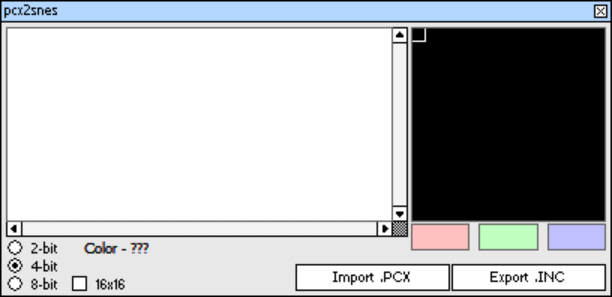
Press Import .PCX, and open tiles.pcx. Then click Export .INC. Save the resulting file as tiles(.inc). Now open up tiles.inc. Change the label "UntitledData" to "Tiles," and "UntitledPalette" to "BG_Palette." All set!
Since we're filling up most of bank 0 with code, let's fill bank 1 with the graphics data. We'll need to put the code in its own section, and we already have the data labeled in tiles.inc in order to get their addresses later.
You generally insert the tile data at the end of your source file. The code will look like this:
.BANK 1
.ORG 0
.SECTION "TileData"

    .INCLUDE "tiles.inc"

.ENDS
Simple, right? Now you need to learn how to upload that palette data.
Now, there are actually 2 ways you can change the palette. You could tell $2121 (CGADD) the color you want to edit, and then write the data from BG_Palette to $2122. The other method is to use DMA. The main advantage to using DMA is that you can load data from any bank, where the first method could only load from the current bank (or maybe you could change the PBR or DBR? Not sure.. But DMA is the best bet). Now, You'll need to learn DMA sometime or another, so you'll learn right now.
DMA (Direct Memory Access)
Note: I strongly encourage that you read Qwertie's section on DMA Transfer Basics, he covers everything perfectly. However, if you have any questions, simply contact me (see Intro for contact info). Do not look at HDMA yet, it's a ways away from this tutorial.
Ok, if you read the section, you now know that there are 8 separate DMA channels, and several registers that need to be written to in order to initialize the DMA. The most confusing of these registers is the DMA Control Register ($43?0). Well, the most confusing bits are the first 3, which determine the transfer type. Let me try to explain it to you after we finish writing the macro code for loading the palette. Let's write some code.
Note: I modeled this after Neviksti's and Marc's palette code. Neviksti's loaded the entire palette, while Marc's allowed you to decide where to begin loading palette data and how many colors to write. I just combined them both. Ok let's go.
;============================================================================
;LoadPalette - Macro that loads palette information into CGRAM
;----------------------------------------------------------------------------
; In: SRC_ADDR -- 24 bit address of source data,
;     START -- Color # to start on,
;     SIZE -- # of COLORS to copy
;----------------------------------------------------------------------------
; Out: None
;----------------------------------------------------------------------------
; Modifies: A,X
; Requires: mem/A = 8 bit, X/Y = 16 bit
;----------------------------------------------------------------------------
.MACRO LoadPalette
    lda #\2
    sta $2121       ; Start at START color
    lda #:\1        ; Using : before the parameter gets its bank.
    ldx #\1         ; Not using : gets the offset address.
    ldy #(\3 * 2)   ; 2 bytes for every color
    jsr DMAPalette
.ENDM

;============================================================================
; DMAPalette -- Load entire palette using DMA
;----------------------------------------------------------------------------
; In: A:X  -- points to the data
;      Y   -- Size of data
;----------------------------------------------------------------------------
; Out: None
;----------------------------------------------------------------------------
; Modifies: none
;----------------------------------------------------------------------------
DMAPalette:
    phb
    php         ; Preserve Registers

    stx $4302   ; Store data offset into DMA source offset
    sta $4304   ; Store data bank into DMA source bank
    sty $4305   ; Store size of data block

    stz $4300   ; Set DMA Mode (byte, normal increment)
    lda #$22    ; Set destination register ($2122 - CGRAM Write)
    sta $4301
    lda #$01    ; Initiate DMA transfer
    sta $420B

    plp
    plb
    rts         ; return from subroutine
It's important to use A for the bank and X for the offset. A is 8-bit, and the bank # is 8 bit, X is 16 bits and the address is 16 bits (well it can be up to anyways). Don't try to load a 16 bit value into an 8 bit register. See what I mean? Also, when you load X into a register when its 16 bits, It loads the low byte into the register you loaded X to, and the high byte into the following register. For example:
ldx #$1122
stx $2000 - stores #$22 into $2000, #$11 into $2001
Whew! Did you absorb all that? I sure hope so, I tried commenting every line so you wouldn't have any questions. If you still don't understand, try reading Qwertie's DMA register references. Yoshi's DMA register descriptions are nice as well.
About the DMA control register. Let's go over all the bits that are sent to this register. I'll use Qwertie's Reference as a guide.
Note: Qwertie mixed up his descriptions for the f and i bits. I corrected that here.
Register $43?0: DMA Control Register (1b/w)
da-ifttt    d: (DMA only)   0=read from CPU memory, write to $21xx registers
                            1=read from $21xx registers, write to CPU memory
            a: (HDMA only)  Don't need to worry about this bit, we're not doing HDMA
            i: 0=increment CPU memory pointer by 1 after every access; 1=decrement
            f: fixed CPU memory address (1=fixed; 0=inc/dec depending on bit i)
            t: DMA/HDMA transfer type

Bit d
  - You can either read from memory and write to $21xx registers, or read from $21xx registers and write to mem. Simple enough..
Bit i
  - inc or dec the DMA source address.
Bit f
  - The DMA source address is either inc/dec'd every read/write, or stays the same.
bit t
  - it can get a little confusing. Look at Qwertie's examples, he has some right below the description of this register.
  - We used transfer type 000. Look at Qwertie's example:

    "The t bits decide the 'mode' of the transfer.
    To describe how this works, suppose the bytes of data to be transferred are $01 $23 $45 $67 $89,
    and the register to write to is $2118.
    Assuming f=0 and i=0:

    Transfer Type           Order of transfer
    000: 1 reg              $01->$2118 $23->$2118 $45->$2118 $67->$2118 $89->$2118
    001: 2 regs             $01->$2118 $23->$2119 $45->$2118 $67->$2119 $89->$2118
    010: 1 reg write twice  $01->$2118 $23->$2118 $45->$2118 $67->$2118 $89->$2118
    011: 2 regs write twice $01->$2118 $23->$2118 $45->$2119 $67->$2119 $89->$2118
    100: 4 regs             $01->$2118 $23->$2119 $45->$211A $67->$211B $89->$2118
    101  unknown behavior
    110  unknown behavior
    111  unknown behavior

    Transfer modes 0 and 2 appear to be the same, but are different in HDMA mode."
Understand? You better!! Do you understand? If not, contact me, I'd be happy to help you out.
Ok that was a lot to take in, but if you still want more, go to Part II to learn how to load your tiles to VRAM.
Go to Working with VRAM [Part 2] - Initializing Tiles and Tile Maps.
Tutorial by bazz